What Is a Printed Circuit Board?
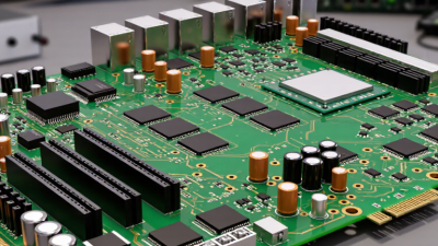
A printed circuit board (PCB) is the flat, often green board that connects and supports electronic components. Copper traces carry signals and power between parts such as processors, resistors, and connectors. The board may look simple. Its layers are not. A typical design combines an insulating substrate, conductive copper, drilled holes, and protective solder mask. Multilayer boards can route dense connections through several copper layers, making compact devices possible. Yet every design involves trade-offs: more layers can save space, but add manufacturing complexity and cost.
The scale of the industry helps explain why this technology matters. Fortune Business Insights’ PCB market report estimated the global market at USD 72.3 billion in 2023 and projected growth to USD 103.7 billion by 2032. These are market estimates, not a measure of product quality. Still, they reflect the board’s role in consumer electronics, vehicles, industrial controls, and communications equipment. Understanding what a printed circuit board does is useful before comparing board types or examining fabrication. A small caveat: a PCB does not make a device reliable by itself. Layout choices, materials, assembly, and testing all matter. Even a neat-looking board can hide a weak connection. This guide introduces the board’s basic structure, common types, and place in modern electronics.
PCB Definition and Function: Interconnecting Electronic Components
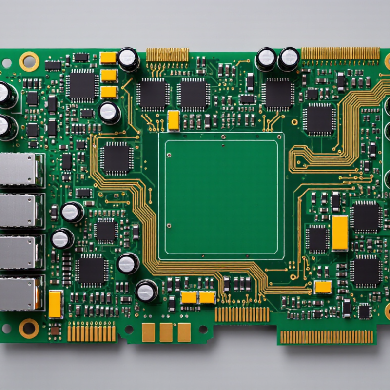
A printed circuit board (PCB) is the platform that holds electronic components in place and connects them electrically. Its insulating base supports thin copper pathways, called traces. These routes carry signals and power between parts such as processors, sensors, and connectors. A board also helps maintain consistent spacing, which matters when components are small or signals move quickly.
Think of a sensor board: copper traces link the sensor to a processor, while holes and solder pads secure the parts. The board’s layout can affect heat flow, signal quality, and repair options. It is more than a mounting surface. Prismark’s 2023 global PCB market data put production value at about $68.4 billion. That figure reflects industry output value, not the number of boards made. WSTS’s Autumn 2024 forecast projected semiconductor sales of $626 billion for 2024, up 19 percent from 2023. Those figures describe related parts of electronics manufacturing, not a direct measure of PCB demand. A useful distinction. More copper layers can support denser connections, but they can also make inspection and repair harder. A PCB design is always a set of trade-offs, and a tidy diagram cannot capture every production challenge.
What Is a Printed Circuit Board?
PCB Definition and Function: Interconnecting Electronic Components
A printed circuit board (PCB) supports electronic components and connects them through conductive copper pathways.
Common stackups use one, two, or multiple copper layers; vias connect pathways between layers.
PCB Structure: Substrate, Copper Layers, Solder Mask, and Legend
A printed circuit board supports components and connects them through patterned copper. Its substrate provides the mechanical base. Many boards use fiberglass-reinforced epoxy, though material choice depends on heat, stiffness, and electrical needs. The board may have one copper layer or several stacked layers. Thin copper traces guide signals and power between component pads. In multilayer designs, plated vias connect traces across layers. Small details matter. Trace width and spacing affect current capacity, signal behavior, and manufacturing yield.
A solder mask is the colored protective coating over much of the copper. It helps prevent solder bridges during assembly, while openings expose pads for component leads. The legend, often called silkscreen, adds printed labels, outlines, and polarity marks. These markings help technicians identify parts and orientation under bright inspection lights. A simple diagram can hide awkward trade-offs: heat, spacing, and manufacturability do not always align. The stackup is not always symmetrical, either. For example, copper distribution and material thickness can influence warping during heating. Clear labels and sensible layer design make a board easier to assemble and inspect, but they cannot fix every design flaw.
PCB Types by Layer Count: Single-, Double-, and Multilayer Boards
What Is a Printed Circuit Board?
PCB Types by Layer Count: Single-, Double-, and Multilayer Boards
A printed circuit board (PCB) holds electronic components and connects them through copper pathways. Its layer count tells you how many conductive copper layers the board uses. A single-layer board has copper on one side of its insulating base. It suits straightforward circuits, such as a basic indicator light, where connections are easy to trace. The layout is simple to inspect, but crowded designs may need more space. Not always.
A double-layer board carries copper on both sides, joined by plated holes called vias. This gives designers more routing options without greatly increasing board size. Multilayer boards stack three or more conductive layers, separated by insulating material. They can fit dense circuits into compact devices, while internal layers carry power or signals. More layers can also make manufacturing and inspection more demanding. The right choice depends on circuit complexity, available space, and production needs—not on layer count alone. In practice, a neat schematic can still become a tricky physical layout.
Tips: Check the board’s routing needs early. If traces must cross often, a single layer may be limiting. Ask a qualified board designer to review layer choices before layout begins.
PCB Copper Weight: 1 oz/ft² Foil Is Approximately 35 μm Thick
A printed circuit board supports electronic parts and connects them through copper paths called traces. Copper weight describes the mass of copper foil spread across a square foot. One ounce per square foot is approximately 35 micrometers thick. That figure is a useful reference, not a precise measurement of every finished board.
Not the whole story.
Manufacturing processes can change the final thickness. Outer copper layers may receive additional copper during plating, while etching removes copper to form traces and gaps. The result depends on the starting foil, plating, and design. A nominal 1 oz/ft² layer may therefore measure differently across a completed panel.
Small differences matter.
They can affect resistance, current capacity, and heat, especially in narrow traces carrying sustained loads. When reviewing a PCB specification, check whether copper weight refers to the starting foil or finished copper. Also consider trace width, layer location, and the expected current.
A thicker copper layer can help reduce resistance, but it may require wider spacing or different etching choices. There is no single thickness that suits every design. I would treat 35 μm as a practical starting point, then verify the finished stack-up with the fabricator. That simple conversion is helpful, though it can hide real process variation.
PCB Fabrication and Qualification: Key Steps and IPC-6012 Classes 1–3
What Is a Printed Circuit Board?
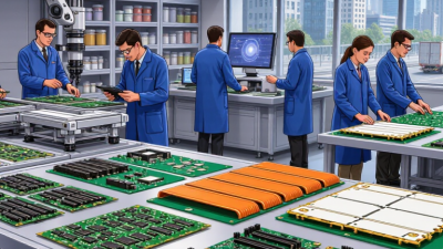
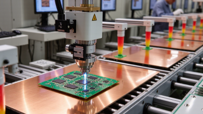
PCB fabrication turns a circuit layout into copper pathways supported by insulating material. Typical steps include imaging, etching, drilling, copper plating, solder-mask application, and surface finishing. Each step can introduce defects: a narrow trace may break, or a plated hole may fail to connect layers. Electrical testing checks continuity and isolation, but inspection and microsection analysis reveal other faults.
Small details matter.
IPC-6012 sets qualification and performance requirements for rigid boards. Class 1 covers general electronic products; Class 2 suits products requiring dependable service; Class 3 applies where continued performance is critical. The right class affects acceptance criteria, inspection, and testing—not just paperwork.
Prismark’s 2024 industry analysis estimated global PCB production at about US$69 billion in 2023, reflecting a market shaped by changing demand and product complexity. That scale makes consistent qualification valuable, but a standard cannot replace clear design requirements or careful supplier review.
A passing test report also cannot prove how a board will perform in every field condition. That deserves attention.