Our Commitment to a Greener Future

A pcb printed circuit board is the quiet foundation inside nearly every electronic product. It supports components, controls electrical connections, and carries signals through carefully designed copper pathways. Look inside a router, medical monitor, or vehicle controller. You will find layered fiberglass, copper foil, solder, and protective coating working together.
The board does more than hold parts in place. Its traces guide power and data between integrated circuits, connectors, sensors, and processors. Vias connect different copper layers through tiny drilled holes. Engineers also manage heat, impedance, noise, spacing, and mechanical stress during design. IPC-2221 provides widely used guidance for printed board design, while IPC’s PCB Technology Roadmap tracks challenges involving high-density interconnects, advanced packaging, and faster signal transmission. These standards show why reliable boards require more than attractive layouts.
Industry data also reveals the board’s growing importance. Prismark’s global PCB market analyses identify expanding demand from automotive electronics, artificial intelligence infrastructure, telecommunications, and consumer devices. SEMI and WSTS reports further show strong long-term pressure for smaller, faster, and more energy-efficient electronic systems. Those systems depend on increasingly capable circuit boards. Yet, a simple diagram can make manufacturing appear effortless. Real boards face drilling variation, solder defects, moisture, contamination, and thermal cycling. That gap matters. Understanding how a pcb printed circuit board works means connecting design theory with inspection, fabrication, assembly, and real-world reliability. Mistakes still happen, even in advanced factories. Careful engineering reduces them, but it never removes the need for testing and reflection.
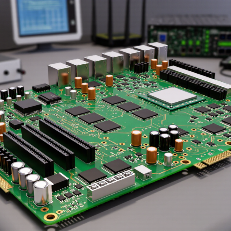
A printed circuit board, or PCB, is the physical foundation of an electronic device. It holds components and connects them through engineered copper pathways. Instead of loose wires, a PCB uses traces, pads, and drilled vias to guide electrical signals across one or more layers.
A typical board contains a rigid or flexible insulating substrate, copper foil, solder mask, and printed markings. The familiar green surface is usually solder mask, not the circuit itself. Underneath, copper traces may be thinner than a strand of hair. Components sit on exposed pads, while vias connect different copper layers through small holes. Power, data, and control signals follow carefully designed routes. Small errors matter.
Market data shows why this structure remains important. The 2024 Prismark PCB industry forecast estimated global PCB sales at roughly 70 billion U.S. dollars in 2023, with continued growth expected through 2028. The IPC PCB Technology Roadmap also links rising density with finer lines, advanced materials, and more complex multilayer construction. These figures describe an expanding industry, but they do not guarantee better design. A crowded board can still suffer from heat, noise, or difficult repairs. In practical inspection, I would check connector alignment, solder quality, and continuity before trusting the assembly. A PCB is not merely a platform. It is a physical map of electrical decisions, and that map sometimes needs questioning.
| Data Dimension | Typical Information | Function or Significance | How It Works in a PCB |
|---|---|---|---|
| Basic Definition | A printed circuit board is a rigid or flexible substrate containing conductive copper patterns. | Provides a physical platform and electrical interconnections for electronic circuits. | Copper traces connect components according to the circuit design. |
| Primary Substrate | Common substrates include glass-reinforced epoxy laminate, polyimide, and other specialized dielectric materials. | Supports copper conductors while electrically isolating different circuit paths. | The insulating material separates conductive layers and helps maintain mechanical strength. |
| Conductive Material | Copper is the standard conductor used for traces, pads, planes, and plated holes. | Offers high electrical conductivity and can be formed into precise circuit patterns. | Electrical current travels through copper features between connected components. |
| Board Structure | PCBs may be single-sided, double-sided, or multilayer. | Determines the available routing area and circuit complexity. | Additional copper layers increase routing capacity while dielectric layers provide insulation. |
| Single-Sided Board | Contains conductive copper on one side of the insulating substrate. | Suitable for relatively simple and low-density circuits. | Components and copper routing are generally arranged around one conductive layer. |
| Double-Sided Board | Contains copper on both sides of the substrate. | Provides more routing space than a single-sided design. | Plated through-holes or vias electrically connect the two copper sides. |
| Multilayer Board | Uses multiple patterned copper layers separated by insulating dielectric layers. | Supports dense, high-speed, and complex electronic designs. | Vias connect selected layers, while internal planes may distribute power or provide a reference path. |
| Copper Trace | A narrow, designed strip of copper that carries an electrical signal or power. | Replaces many individual wires in a compact circuit assembly. | Trace width, thickness, spacing, and length affect current capacity and signal behavior. |
| Power Plane | A broad copper area connected to a power potential. | Distributes power with lower impedance than narrow routing in many designs. | Components connect to the plane through vias, pads, or short traces. |
| Ground Plane | A broad copper area connected to the circuit reference or ground network. | Provides a return-current path and can help reduce electromagnetic interference. | Signals reference the ground structure, and current returns through an appropriately designed path. |
| Via | A plated hole or micro-scale interconnection that links copper layers. | Allows routing to move vertically through a multilayer board. | The conductive barrel or structure creates an electrical connection between selected layers. |
| Through-Hole | A component lead passes through a drilled hole and is soldered to a pad. | Provides strong mechanical retention and electrical connection. | The component lead occupies a hole that may be connected to one or more copper layers. |
| Surface-Mount Pad | A copper landing area designed for a component terminal mounted on the board surface. | Enables compact assembly and high component density. | Solder bonds the component terminal to the pad and completes the electrical connection. |
| Solder Mask | A protective polymer coating applied over most exposed copper. | Helps prevent solder bridges, oxidation, and accidental short circuits. | Openings in the coating expose only the pads and other areas that require soldering or contact. |
| Component Legend | Printed markings identify reference designators, polarity, pin locations, and assembly information. | Assists inspection, assembly, repair, and troubleshooting. | Markings are placed on the board surface without forming part of the conductive circuit. |
| Surface Finish | A metallic finish protects exposed copper pads and improves solderability. | Reduces oxidation during storage and assembly. | The finish forms the final exposed surface on pads, contacts, and selected plated features. |
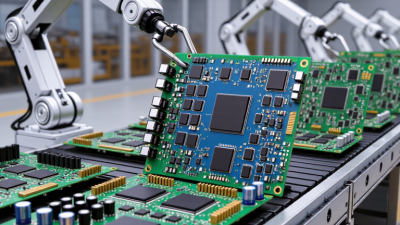
| Electrical Components | Examples include resistors, capacitors, inductors, diodes, transistors, and integrated circuits. | Perform functions such as resistance, energy storage, switching, amplification, and computation. | Components are electrically connected through pads, traces, vias, and planes. |
| Signal Routing | Routes are arranged to connect circuit nodes while meeting spacing, length, and impedance requirements. | Maintains intended electrical performance and reduces unwanted coupling. | Design software defines the path between component terminals and verifies design rules. |
| Thermal Management | Copper areas, thermal vias, heat-spreading layers, and external cooling structures may be used. | Moves heat away from components and helps maintain safe operating temperatures. | Heat conducts through copper and substrate structures before being transferred to the surrounding environment. |
| PCB Design Files | Design data normally describes board geometry, copper layers, drilling, solder mask, markings, and component placement. | Provides manufacturing and assembly instructions. | Fabrication data defines the bare board, while assembly data identifies component locations and orientations. |
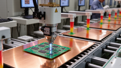
| Manufacturing Sequence | Typical stages include imaging, etching, drilling, plating, lamination, solder-mask application, finishing, and inspection. | Converts the digital circuit layout into a physical board. | Each process forms or protects a specific mechanical or electrical feature. |
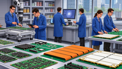
| Testing Methods | Common checks include visual inspection, electrical continuity testing, isolation testing, and functional testing. | Detects manufacturing defects and confirms that intended connections operate correctly. | Test equipment compares the finished board with design requirements and expected electrical behavior. |
| Main Advantages | Compact wiring, repeatable construction, reduced assembly complexity, and support for high component density. | Improves reliability and enables consistent production of electronic devices. | The board integrates mechanical support, electrical interconnection, and thermal features into one assembly platform. |