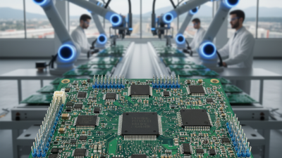
What Is PCB Board Manufacturing and How Does It Work?
A printed circuit board may look like a thin green sheet, but it is the physical foundation of modern electronics. PCB board manufacturing turns a design file into a tested electrical platform. Copper traces carry signals between components. Vias connect different layers. Solder masks protect exposed conductors, while silkscreen markings guide assembly and inspection.
Dr. Paul Eisler, widely recognized as a pioneer of the printed circuit, described its importance simply: “The printed circuit is the basis of modern electronics.” His observation still fits today’s factories. A typical production line may begin with copper-clad laminate and continue through imaging, etching, drilling, plating, solder-mask coating, and electrical testing. Each stage demands careful control. A small alignment error can interrupt a high-speed signal. A poorly plated hole can fail after repeated thermal cycles.
The process is precise, but never perfect. That matters. Engineers must review tolerances, material choices, surface finishes, and manufacturability before production starts. Operators also inspect real panels, not only digital drawings. Dust, heat, chemical balance, and tool wear can change results.
This guide explains how PCB board manufacturing works, from raw laminate preparation to final quality checks. It also examines common defects, production costs, and design decisions that affect reliability. The goal is practical understanding, not factory jargon. A circuit board should not merely function on the bench. It should remain stable inside the product, under real pressure, vibration, moisture, and time.
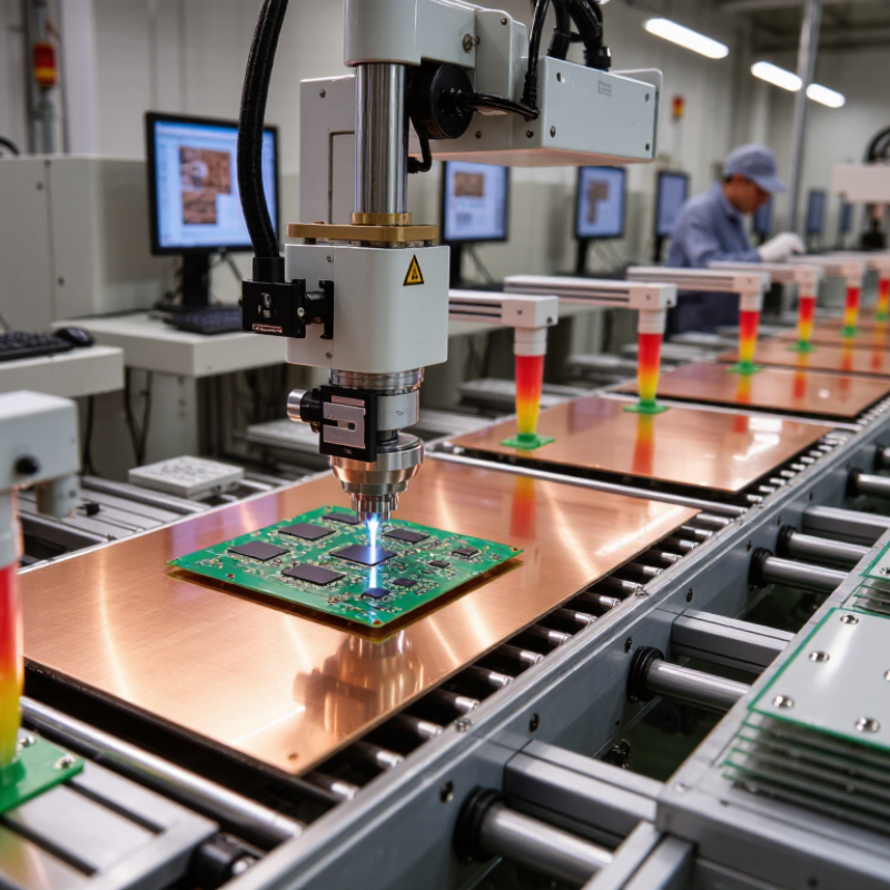
PCB Manufacturing Defined: From Bare Board to Functional Circuit
What Is PCB Board Manufacturing and How Does It Work?
PCB manufacturing turns an electrical design into a layered, testable structure. The process begins with copper-clad laminate, often reinforced with fiberglass for strength and stability. Design files define traces, holes, component locations, and layer connections. Engineers check spacing and signal paths before production starts. Small errors here can multiply later. That part is easy to underestimate.
The bare board passes through imaging, etching, drilling, and copper plating. Imaging transfers the circuit pattern onto the copper surface. Etching removes unwanted copper and leaves precise conductive paths. Drilling creates holes for component leads and connections between layers. Plating strengthens these holes and improves electrical continuity. A solder mask then protects exposed copper, while printed markings identify component positions. The process is less tidy than diagrams suggest. Dust, heat, and alignment changes can affect results.
Inspection follows every major stage, not only the final one. Automated checks can detect missing traces, short circuits, and incorrect hole sizes. Technicians may also examine surface finish and board flatness. After fabrication, components are placed and soldered onto the board. Functional testing applies power and checks whether signals reach the expected points. A board can look perfect and still fail under temperature or vibration. That is why reliable production depends on measured tolerances, documented checks, and careful review of real test data.
Material Selection and Layer Design: 1.6 mm Boards with 18 µm Copper Foil
PCB board manufacturing begins with material choices that influence every later process. For many two-layer boards, a 1.6 mm FR-4 laminate provides practical stiffness and manageable drilling. The 18 µm copper foil starts as a thin conductive layer. Plating may increase its finished thickness around holes and exposed areas.
Layer design must match the circuit’s electrical and mechanical demands. Trace width, spacing, and copper weight affect current capacity and heat release. High-speed signals also need a controlled distance from their reference plane. A careless stack-up can create unwanted impedance changes. Small errors matter. Designers should reserve space for vias, solder mask clearance, and component tolerances.
Manufacturing usually includes imaging, etching, drilling, copper plating, solder mask application, and electrical testing. During etching, narrow traces can lose more copper than expected. Uneven copper distribution may also cause plating differences across the panel. Production reviews often use test coupons and cross-section checks to verify hole walls, insulation thickness, and finished copper. Thermal cycling remains important, especially when the board connects to heavy components.
Drawings can mislead. A layout may look perfect but leave no room for fabrication variation. Material data should be checked against the actual laminate batch, not only a standard datasheet. Reviewing drill-to-copper spacing and panel movement early can prevent expensive rework. Some designs still need refinement after the first prototype, and that is normal engineering practice.
Imaging, Etching, and Plating: Forming 0.1 mm Class Conductive Features
What Is PCB Board Manufacturing and How Does It Work?
PCB manufacturing turns a copper-clad panel into a controlled electrical structure. Prismark’s 2024 industry forecast estimated global PCB production at about US$73 billion in 2023. Fine-line capability now matters more as devices shrink. A 0.1 mm feature is roughly four mils wide. It leaves little room for process drift.
Imaging transfers the circuit pattern onto dry film, often with laser direct imaging. The machine exposes selected areas on a clean, flat panel. Etching removes unwanted copper, but chemical attack can narrow lines and create undercutting. Plating then restores copper thickness on exposed traces and inside drilled holes. A typical 35 μm copper layer can require tight control of current density, temperature, and bath chemistry. IPC-2221C and IPC-6012E provide design and qualification guidance, while IPC technology trend studies identify fine-line control as a growing production priority. In practice, 0.1 mm results are never guaranteed by artwork alone. That is the uncomfortable part.
Tips:
Keep imaging-room humidity stable, verify exposure with test coupons, and measure line width after etching. Do not trust a single inspection point. Compare panel center and edges. Track etch factor, plating thickness, and registration together. A process can pass one measurement and still fail after thermal stress. Small deviations become visible under a microscope. Manual review still catches mistakes.
Drilling, Lamination, and HDI Fabrication with Microvias Below 150 µm
PCB board manufacturing turns an electrical design into a layered physical structure. HDI boards require tighter control than conventional multilayer boards. Fabricators begin with copper-clad cores, imaging, etching, and controlled drilling. Every hole must match the stack-up. Small errors accumulate quickly. A 100 µm microvia is not simply a smaller hole. It changes material selection, laser settings, desmear chemistry, and inspection methods. Keep that in mind.
Mechanical drills create larger through-holes, while laser drills form blind microvias between adjacent layers. The laser removes dielectric above a copper target without cutting too deeply into it. Operators check hole diameter, taper, depth, and copper exposure. Resin smear can block electrical contact. Desmear treatment removes residue, but excessive treatment can weaken the interface. Lamination then presses dielectric sheets and copper foils under heat and pressure. The press cycle must control temperature rise, pressure profile, and cooling. Warpage is a practical concern, not just a drawing note.
For microvias below 150 µm, sequential build-up often repeats laser drilling, copper filling, imaging, and lamination. Electroplated copper fills the cavity and supports stacked or staggered connections. HDI fabrication relies on registration accuracy across every build-up cycle. Automated optical inspection, cross-sections, and electrical tests reveal voids, cracks, and misalignment. Yet inspection is not infallible. A clean report can still miss a weakness that appears after thermal cycling. Reliable production links design rules with process records, sample testing, and engineering review.
Inspection and Testing: IPC-6012 Compliance, AOI, and Electrical Verification
PCB board manufacturing depends on disciplined inspection, not visual confidence.
IPC-6012 defines qualification and performance requirements for rigid printed boards, including materials, construction, and test expectations. The standard supports three performance classes, allowing requirements to match product risk. A 2024 IPC North American PCB Statistical Program report tracks monthly sales, bookings, and book-to-bill ratios. That data shows why stable inspection controls matter when production demand shifts.
Automated optical inspection examines copper patterns, solder masks, pads, holes, and spacing.
Cameras compare each board with approved design data. Operators then review flagged areas, such as a thin trace near a plated hole. Small defects matter. AOI improves repeatability, but it cannot confirm hidden electrical continuity. It may also misread glare, contamination, or uneven solder mask. That gap matters.
Electrical verification checks nets for continuity and unwanted connections.
Flying-probe systems suit prototypes and varied batches, while fixture-based testing supports higher volume. Test records should identify board revision, probe program, limits, and operator approval. IPC-6012 compliance also requires documented evidence, not verbal assurance. In practice, experienced engineers correlate AOI findings with cross-section analysis and resistance measurements. The process is not perfect. A missed false negative should trigger a review of lighting, sampling, and test coverage. Calibration records and traceable instruments strengthen reliability during customer audits.