Navigating the PCB fabrication and assembly process can be complex and challenging. According to industry reports, the global PCB market is projected to reach $80 billion by 2026. This growth stresses the importance of efficiency in manufacturing. John Smith, a leading expert in PCB technology, stated, “A precise approach to fabrication can significantly enhance product reliability.” His insight highlights the critical importance of understanding each stage of the process.
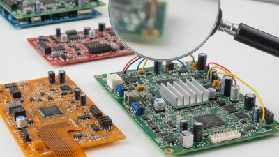
The PCB fabrication and assembly landscape continually evolves. Technologies improve, and materials develop. However, many companies still struggle with quality control. Frequent errors can lead to delays and increased costs. Aligning with reliable suppliers who understand these challenges can mitigate risks. Understanding both fabrication and assembly is vital for achieving high-quality output.
Fostering collaboration between designers and manufacturers is crucial. This approach can resolve potential issues before they escalate. Companies must also invest in training their teams. Adapting to changes in technology is not optional but necessary. Failing to evolve can hinder progress in an increasingly competitive marketplace. Addressing these aspects will ensure a smoother journey through PCB fabrication and assembly.
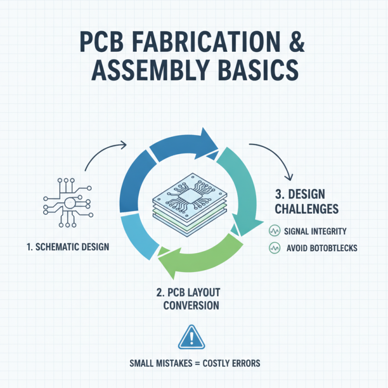
The fabrication and assembly process of printed circuit boards (PCBs) is intricate and demanding. Understanding its basics is crucial for anyone involved. It starts with designing the schematic and converting it into a PCB layout. Designers face challenges at this stage, like ensuring signal integrity and avoiding bottlenecks. Even small mistakes can lead to costly errors later.
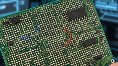
Once the design is complete, the fabrication process begins. This phase includes etching copper layers and applying solder masks. Manufacturers must maintain high standards to ensure quality. However, variations in materials or processes sometimes occur, which can affect outcomes. Testing the fabricated boards can uncover defects. Not all tests yield clear results, leading to unpredictability in assembly.
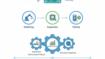
The assembly of the PCB follows fabrication. This stage often involves soldering components onto the board. Various methods exist, such as surface mount technology and through-hole assembly. Each has advantages and challenges. Assembly can suffer delays due to component shortages or incorrect placements. Keeping track of parts and revisions requires organization. It's a complex journey, filled with learning opportunities and room for improvement.
The PCB design process involves several key stages that are crucial for successful fabrication and assembly. At the outset, the design schematic is developed. This phase entails defining the circuit layout and component interactions. According to industry reports, a well-executed schematic can reduce errors by up to 40%. This emphasizes the need for clear, precise designs.
Next, the PCB layout is created. This involves placing components on the board and routing connections. A study by IPC shows that optimizing the layout can improve manufacturing yields by 25%. Designers often underestimate the complexity of this stage, leading to potential delays and additional costs.
After the layout phase, prototypes are manufactured. Testing these prototypes is essential. Approximately 70% of design flaws are caught during this testing. However, many projects face unexpected challenges at this point. Issues like component misalignment or signal integrity problems can arise, requiring careful revisions. Each stage has its pitfalls, which makes attention to detail paramount in the PCB design process.
This chart illustrates the key stages in the PCB design process, highlighting the time spent on each phase.
When considering PCB manufacturing, selecting the right materials is crucial. Common substrates include FR-4, a fiberglass material, due to its excellent insulation properties. However, other options exist. For high-frequency applications, polyimide may be more suitable. Each material has its own pros and cons. Understanding these can enhance your design's performance.
In addition to substrates, the choice of copper thickness significantly affects the PCB’s conductivity. Thicker copper can handle higher currents but may complicate the etching process. Moreover, solder mask and silkscreen inks are essential for protecting the PCB and ensuring proper labeling, respectively.
Tools required for PCB assembly include soldering equipment and inspection tools. A soldering iron or hot air rework station can aid in component attachment. For quality assurance, proper inspection tools must be used to check for solder joints and alignment. However, users should remain aware of common pitfalls, such as inadequate cleaning of materials, which can lead to poor adhesion or circuit failure. Experimenting with different setups is often necessary to truly find what works best for your specific needs.
Quality control in PCB assembly is crucial for delivering reliable products. To achieve high standards, implement structured processes from the start. Begin by selecting materials that meet your specifications. Use only components that comply with industry standards. This proactive approach helps prevent defects later on.
Monitoring the assembly process is vital. Regularly inspect solder joints and connections. Use automated optical inspection (AOI) systems for quick and accurate assessments. Train your staff to recognize common errors. Human oversight is essential, but machines can help catch many mistakes.
Tips: Establish a clear protocol for addressing defects. Document issues thoroughly. Foster a culture of continuous improvement, encouraging feedback from team members. This promotes a collaborative environment where everyone aims for excellence. Don't overlook the importance of post-assembly testing. Even minor flaws can lead to major issues in the field. Regular audits can ensure compliance with best practices.
Effective communication with PCB manufacturers and suppliers is crucial for successful fabrication and assembly. Clear, concise messages help avoid misunderstandings. Start with well-defined specifications. Outline your expectations regarding materials, dimensions, and timelines. Be specific about your requirements to minimize back-and-forth communication.
Establish a comfortable level of engagement with your suppliers. Ask questions and encourage them to share their insights. This collaboration fosters trust and enhances the project's overall success. Feedback should be constructive, highlighting areas for improvement. Acknowledge potential challenges. Sometimes, solutions may not match your initial vision. Embrace flexibility and be open to alternatives. This can lead to innovative outcomes you might not have considered.
Stay organized and maintain a detailed record of communications. Use project management tools to track progress. This not only shows professionalism but also helps in addressing issues swiftly. Miscommunication can lead to delays, so keep lines of communication open. Remember, effective dialogue is a two-way street where learning and adaptation are key.
| Communication Aspect | Tips | Importance |
|---|---|---|
| Clear Specifications | Provide detailed drawings and specifications. | Ensures accurate manufacturing. |
| Regular Updates | Request frequent progress reports. | Maintains transparency in the process. |
| Open Feedback | Encourage questions and feedback from the manufacturer. | Improves collaboration and outcomes. |
| Sample Reviews | Request prototypes or samples before full production. | Identifies potential issues early on. |
| Timeline Management | Establish clear timelines and deadlines. | Helps to meet project milestones. |
| Quality Control | Set clear quality standards and expectations. | Ensures the reliability of the final product. |