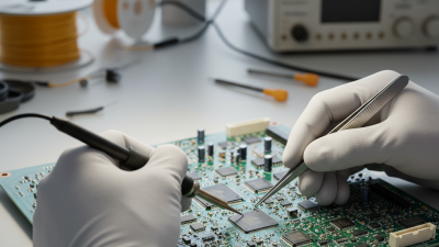
A finished electronic product may look clean and simple from the outside. Inside, however, tiny components must connect reliably across a carefully designed board. Printed circuit board assembly, often shortened to PCBA, is the process of mounting and joining those components to a bare printed circuit board. It turns a pattern of copper tracks into a working electronic assembly. Small details matter.
Dr. Eric Bogatin, a respected educator in PCB design and signal integrity, offers a useful principle: “Interconnections shape performance.” This is a concise paraphrase of his teaching, not a verbatim quotation. It captures why assembly quality depends on more than placing parts in the right spots. Solder joints, component orientation, temperature control, and inspection all affect whether a board behaves as intended. A misaligned connector or a weak joint can stop an otherwise well-designed device from working.
The process often begins with solder paste applied through a stencil. Pick-and-place machines position components, then a reflow oven heats the board so solder forms electrical and mechanical connections. Through-hole parts may require a separate soldering step. Technicians and automated inspection systems check for missing parts, bridges, and other defects. The exact sequence varies with the design and production volume.
Assembly is precise, but never entirely automatic in the human sense. Engineers still make choices, and some trade-offs are less obvious than they first appear. A fast process is not always the most reliable one. Understanding each stage helps readers evaluate how a board is built, tested, and improved—and where careful review can still make a difference.
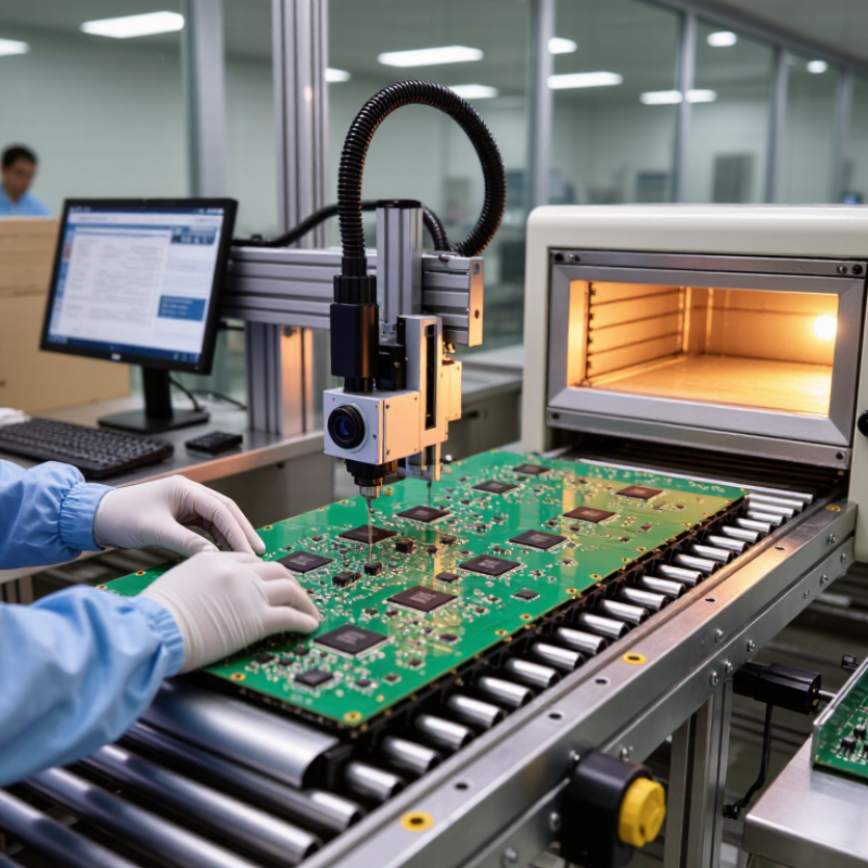
Printed circuit board assembly, or PCBA, means fitting and soldering electronic components onto a bare circuit board. The bare board provides copper pathways; the components perform functions such as storing data, sensing temperature, or controlling power. During surface-mount assembly, a printer lays solder paste onto small pads. Pick-and-place equipment positions parts, then a reflow oven melts the solder. Larger connectors may be fitted through drilled holes and wave-soldered. The result is a working electronic subassembly, not just a green board.
Prismark’s 2024 industry forecast placed global PCB production value near US$73 billion for 2024, following a downturn in 2023. That figure concerns boards, not the full value of assembled products. It still shows the scale of the platform beneath everyday electronics. Assembly quality depends on details: paste volume, component alignment, heat profile, and clean solder joints. Inspectors use magnification and automated optical inspection; electrical tests can reveal open connections or shorts. IPC-A-610 provides widely used criteria for judging electronic assembly acceptability. Yet passing inspection does not prove every product will perform perfectly in its final environment. A board can meet visual criteria and still need careful functional testing. That distinction matters.
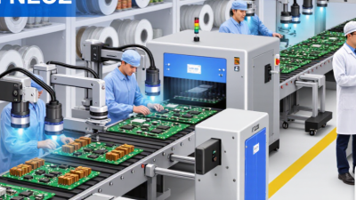
A PCB assembly begins with a bare printed circuit board: a rigid or flexible base carrying thin copper pathways. These traces connect components without loose wires. Copper layers may sit on one or both sides, separated by insulating material. Small drilled holes allow parts or electrical connections to pass through the board.
The components do different jobs. Resistors limit current, capacitors store and release energy, and integrated circuits process signals or control functions. Diodes guide current in a preferred direction. Connectors link the board to cables, batteries, or other assemblies. Some designs also use switches, sensors, heat sinks, or metal shields. The exact mix depends on the device.
Solder joints hold components in place and create electrical connections. Surface-mounted parts sit directly on copper pads; through-hole parts have leads inserted into drilled holes. During assembly, solder is heated until it bonds the metal surfaces. A poorly formed joint can look dull or uneven, though appearance alone does not prove a fault. Inspection and electrical testing provide better evidence. Labels printed on the board can help technicians identify parts, but dense layouts sometimes make them hard to read. Small details matter. A misplaced connector or reversed component may stop the whole board from working.
| Part or Material | What It Is | Role in the Assembly | How It Is Typically Assembled |
|---|---|---|---|
| Bare printed circuit board (PCB) | An insulating substrate with patterned copper layers, conductive traces, and component pads. | Supports components and provides electrical pathways between them. | Serves as the foundation; components are attached to its pads or inserted through its holes. |
| Electronic components | Parts such as resistors, capacitors, diodes, transistors, and integrated circuits. | Perform functions such as processing signals, storing charge, switching, and regulating current or voltage. | Mounted on the board surface, inserted through holes, or assembled using a combination of both methods. |
| Solder paste | A mixture of fine solder alloy particles and flux. | Temporarily holds surface-mount components in position and forms electrical and mechanical joints during reflow. | Usually deposited onto surface-mount pads through a stencil before components are placed. |
| Solder joints | Solidified solder connecting component leads or terminals to PCB pads or plated holes. | Create electrical connections and help secure components to the board. | Formed by reflow soldering for many surface-mount parts or by wave, selective, or hand soldering for through-hole parts. |
| Connectors and electromechanical parts | Items such as board connectors, switches, relays, and sockets. | Provide external connections or mechanical functions, such as switching or interfacing with other assemblies. | May use surface-mount terminals, through-hole leads, or mechanical fasteners, depending on the part design. |
| Solder mask and silkscreen | Protective coating over much of the copper surface and printed markings on the board. | The solder mask helps limit solder bridging; silkscreen markings identify components, polarity, and reference locations. | Typically applied during PCB fabrication, before component assembly. |
| Thermal-management parts | Heat sinks, thermal pads, or other heat-transfer materials used where required by the design. | Help transfer heat away from components that generate significant heat. | Attached or installed according to the component and board design; not present on every assembly. |
| Inspection and test points | Accessible pads, test features, or designated locations used during manufacturing checks. | Support checks for assembly quality and electrical operation. | Used with visual inspection, automated optical inspection, or electrical testing as specified for the product. |
A PCB assembly (PCBA) is a fabricated circuit board populated with components and joined by solder or other specified attachment methods. Its exact parts and assembly steps depend on the circuit design.
Before components are fitted, the bare printed circuit board is checked for damage, contamination, and dimensional accuracy. Technicians compare its outline, thickness, and hole locations with the assembly data. They also inspect the copper pads and solder mask under good lighting. Scratches, lifted pads, or blocked holes can cause trouble later. Details matter. A board that looks clean may still carry residues that interfere with soldering, so cleaning and drying should follow the board material and process requirements.
Next, the board is prepared for accurate placement. Fiducial marks give automated equipment reference points, while tooling holes help hold the panel steady. The assembly team confirms the board revision and checks that its surface finish is suitable for the planned soldering process. If moisture exposure is a concern, handling and storage instructions should be reviewed rather than applying heat by habit. That detail is easy to underestimate. A final inspection checks panel orientation and confirms that solder paste openings will align with the pads. Visual checks help, but they cannot reveal every hidden defect; that is why preparation also depends on controlled process records and appropriate testing.
Component placement begins with a solder paste stencil, which deposits small amounts of paste onto copper pads. The paste should look even, not smeared across neighboring pads. A pick-and-place machine then uses board data and vision cameras to position surface-mount components. Tiny resistors may sit beside larger chips, so accurate alignment matters. A slight shift can cause weak joints or electrical shorts. Small parts are less forgiving.
Next, the board travels through a reflow oven. Heat melts the paste, then controlled cooling forms solder joints. The temperature profile must suit the board and its components; too much heat can damage parts, while too little may leave unreliable connections. Through-hole components follow a different path. Their leads pass through drilled holes and are soldered by selective or wave soldering, or by hand for small runs. It is not foolproof. Inspection checks placement and joints, often with cameras and, when needed, X-ray imaging. Operators may still find defects that automated checks miss. Paste volume, board cleanliness, and component handling all affect the result. A process sheet helps, but real boards sometimes reveal details the setup did not anticipate.
A completed printed circuit board assembly is inspected before it is treated as ready for use. Technicians check component placement, solder joints, polarity marks, and the board’s edges under bright lighting. Automated optical inspection can flag shifted parts or uneven solder, but it cannot see every hidden connection. X-ray imaging helps examine joints beneath packages such as ball-grid arrays. Small details matter: a solder bridge may look like a silver thread, while a lifted component can cast a faint shadow.
Inspection is followed by electrical and functional tests selected for the board’s design. In-circuit testing checks for shorts, opens, and component values; flying probes can serve smaller production runs without a custom fixture. A powered test may confirm that indicators light, sensors respond, or communication signals stay within specified limits. Test results should be recorded with board identifiers and clear pass criteria. A fixture can also create misleading failures if its contacts are worn or misaligned. That possibility deserves attention. No single test proves a board will never fail, so teams review defects, correct the process, and retest repaired assemblies before release.