What is PCB Fab and How Does it Impact Electronics?
The world of electronics heavily relies on PCB fab. This term refers to the process of manufacturing printed circuit boards. PCB fab plays a crucial role in the functionality and efficiency of electronic devices.
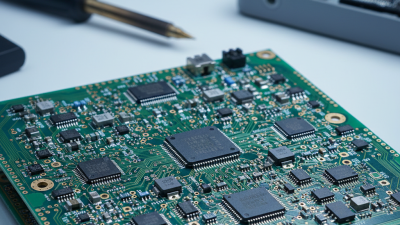
Every electronic gadget, from smartphones to computers, depends on these boards. They connect the various components, allowing signals to flow. Without proper PCB fabrication, devices can malfunction or underperform. The process involves various techniques and materials, reflecting the complexities of modern technology.
However, PCB fab is not without its challenges. Issues such as design errors and production flaws can arise. These shortcomings can lead to significant delays and increased costs. Reflecting on these imperfections can help us improve the industry standards. Ultimately, understanding PCB fab is essential for innovation in the electronics sector.
What is PCB Fabrication (PCB Fab)?
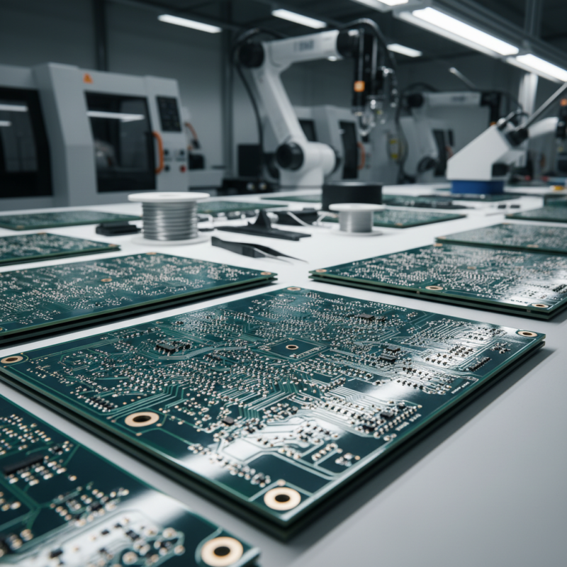
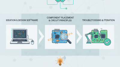
PCB fabrication, or PCB fab, is the process of creating printed circuit boards. This involves several steps, from designing the layout to etching the materials. The layout is often designed using specialized software. This design is crucial because it determines how components will be arranged and connected. Mistakes in this stage can cause major issues later.
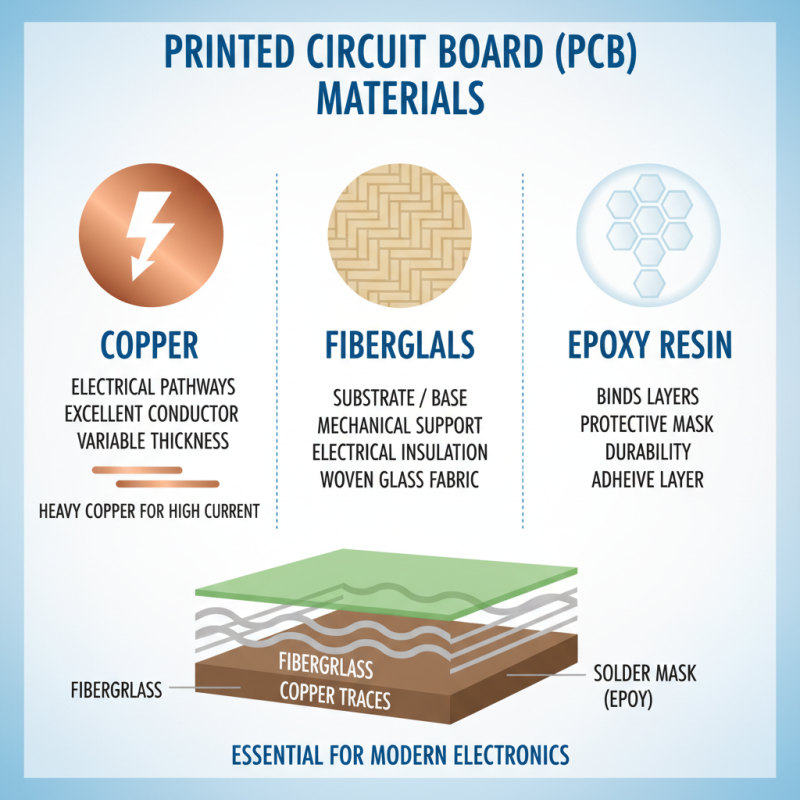
The fabrication stage includes several techniques such as layering, etching, and drilling. Materials like copper and fiberglass are used to create the board. During etching, unwanted copper is removed, leaving behind the desired connections. This part of the process requires precision. Even slight errors can lead to malfunctioning circuits.
After fabrication, the boards undergo testing. This is an essential step because it verifies functionality. Some boards may pass visual inspections but fail electrical tests. Thus, attention to detail in the initial fabrication can save time. A small oversight in design can lead to significant challenges in electronics.
Impact of PCB Fabrication on Electronics
The PCB Fabrication Process Explained
The PCB fabrication process is vital for modern electronics. It involves several steps, starting from design to manufacturing. A report by the IPC states that the global PCB market is forecast to reach $79 billion by 2024. This growth shows the importance of PCBs in various sectors, including automotive and consumer electronics.
During fabrication, designers create layouts that are then translated into circuit boards. This includes etching copper patterns onto a substrate. Mistakes here can lead to significant issues. Each layer must be precise and properly aligned. According to a recent study, about 30% of PCBs manufactured encounter issues during assembly. Addressing these errors is crucial to ensure quality.
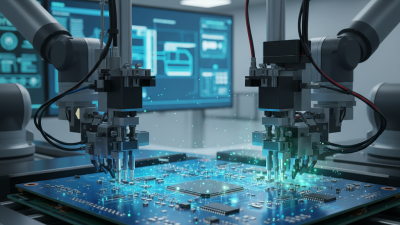
After the boards are created, components are soldered onto them. This step demands high precision. The soldering process can introduce defects like cold solder joints. It’s an area needing constant improvement. Technologies like automated optical inspection (AOI) help detect flaws post-manufacturing. However, not all issues can be spotted. Continuous advancements in technology are necessary to enhance yields and reduce waste in the PCB industry.
What is PCB Fab and How Does it Impact Electronics? - The PCB Fabrication Process Explained
| Dimension |
Description |
Impact on Electronics |
| Layer Count |
Number of conductive layers in the PCB |
Increases complexity and allows for more connections |
| Base Material |
Material used as the substrate for the PCB |
Affects electrical performance and reliability |
| Board Thickness |
Thickness of the PCB material |
Influences the overall strength and durability |
| Copper Weight |
Amount of copper used for traces |
Determines current-carrying capacity and thermal performance |
| Surface Finish |
Coating applied to exposed copper areas |
Protects against oxidation and improves solderability |
| Drill Size |
Size and precision of drilled holes |
Affects component fit and electrical connectivity |
The Role of PCB Fab in Electronic Device Functionality
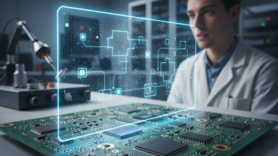
The role of PCB fabrication, or PCB fab, is crucial in the world of electronics. It directly impacts how various devices function. Printed circuit boards are the backbone of electronic products. They connect components and allow electricity to flow. Without efficient PCB fabrication, devices might fail to operate as intended.
One major aspect of PCB fab is precision. Each detail on the board must be accurate. Even a small misalignment can lead to significant issues. Components may not fit properly, or connections may fail. Engineers often face challenges in achieving the right balance of quality and cost. It’s a continuous learning process. Innovations in fabrication methods push the boundaries but introduce new hurdles to overcome.
Furthermore, the choice of materials in PCB fabrication is vital. Different materials affect the board's thermal management and signal integrity. Choosing the wrong type can diminish a device's performance. It's not always straightforward. Designers must reflect on trade-offs between various properties. As technology advances, the ability to adapt PCB designs becomes even more significant for functionality and reliability.
Future Trends in PCB Fabrication Technology
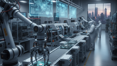
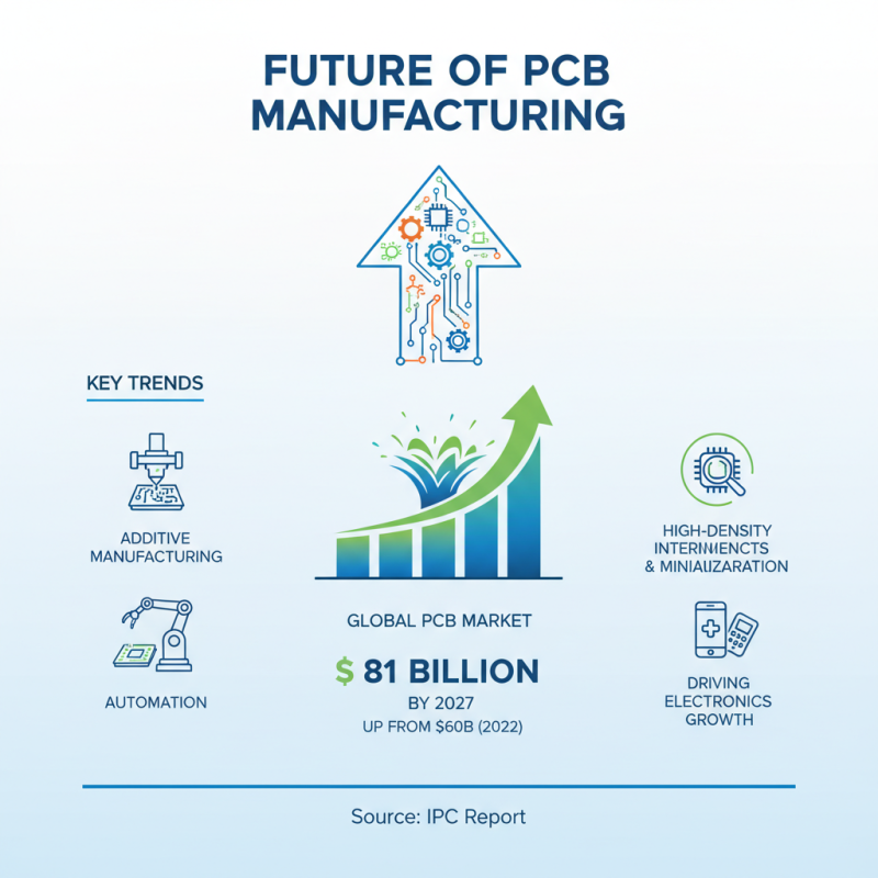
The landscape of PCB fabrication is rapidly changing. Emerging technologies like additive manufacturing and automation are leading this shift. A report from IPC states that the global PCB market is expected to reach $81 billion by 2027. This growth is driven by the demand for high-density interconnects and miniaturization in electronics.
Additive manufacturing provides an innovative approach to PCB production. It allows for more complex designs and reduces material waste. However, challenges remain in achieving consistent quality and scalability. Traditional methods are still predominant, but they face pressure to innovate.
Moreover, automation plays a crucial role. As labor costs rise, companies are turning to automated processes to enhance efficiency. A study by Research and Markets indicates that the automation market for PCB manufacturing is projected to grow by over 15% annually. Yet, the industry must address the skills gap. There is a need for skilled workers who understand these advanced technologies. Balancing innovation with workforce capabilities will be essential for future success.