2026 How to Master PCB Board Design for Beginners?
In the world of electronics, mastering PCB board design is crucial for success. Renowned expert Dr. Emily Chen, a leading figure in this field, once stated, "Effective PCB design bridges ideas with reality." Her words resonate throughout the industry, underscoring the significance of grasping core principles in this area.
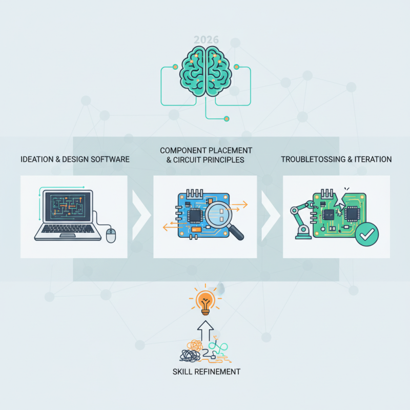
Beginners often face challenges when diving into PCB board design. They struggle with software complexities and component placement. It's not simply about creating a layout; it involves understanding the flow of electricity and the fundamentals of circuit behavior. Errors such as improper trace widths or inadequate spacing can lead to circuit failures.
At times, beginners can feel overwhelmed. The vast array of tools and techniques can be daunting. Reflection upon these experiences is essential for growth. Mistakes made during the design process often teach the most valuable lessons. Embracing these challenges will ultimately refine your skills in PCB board design.
Understanding PCB Design Fundamentals and Terminology
When starting with PCB design, understanding basic terminology is crucial. A PCB, or printed circuit board, serves as the backbone of electronic devices. It consists of layers of conductive and insulating materials. Each layer has specific functions, and knowing these can help in creating efficient designs.
Common terms include trace, pad, and vias. Traces are copper pathways that connect different components. Pads are the small areas where components are mounted. Vias allow connections between different layers. It might seem simple, but miscalculating trace width can lead to issues. Proper sizing is essential for current handling and performance.
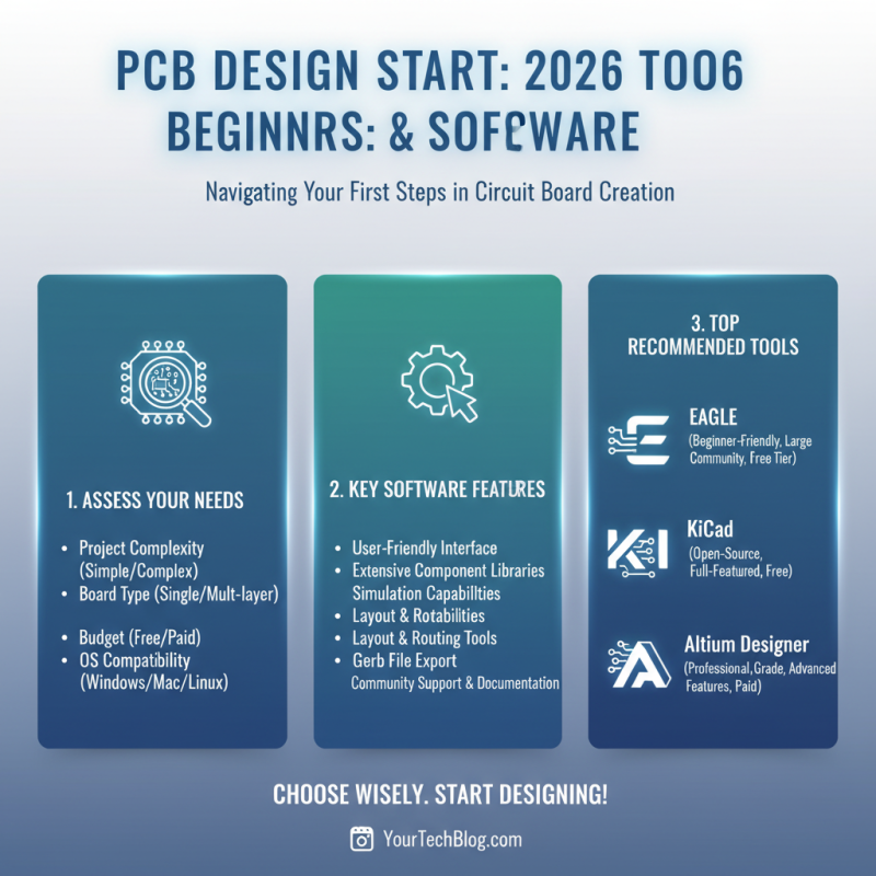
Design software can be overwhelming for beginners. It’s easy to feel lost in the multitude of features and functions. Many software platforms leave users grappling with complex interfaces. Mistakes in layout can happen, from misplaced components to incorrect connections. Learning from these errors is part of the journey. Practice is key, and reviewing fundamental concepts often helps reinforce your knowledge.
2026 How to Master PCB Board Design for Beginners? - Understanding PCB Design Fundamentals and Terminology
| Dimension |
Description |
Importance |
Recommended Tools |
| Schematic Design |
Initial step of PCB design where the circuit is diagrammatically drawn. |
Essential for visualizing the circuit connections. |
Eagle, KiCAD |
| Layout Design |
Arranging components on the PCB to ensure optimal performance and manufacturability. |
Crucial for minimizing noise and ensuring signal integrity. |
Altium Designer, OrCAD |
| DRC (Design Rule Check) |
A process to verify that design complies with manufacturing constraints. |
Helps avoid production issues and improves reliability. |
Mentor Graphics, PCB Artist |
| PCB Fabrication |
The process of producing the physical PCB from the design files. |
Vital for turning designs into tangible products. |
Gerber Viewer |
| Component Selection |
Choosing appropriate electronic components based on specifications and availability. |
Directly impacts cost, performance, and size of the PCB. |
Mouser, Digi-Key |
Key Design Principles: Layer Stacking and Signal Integrity
When designing PCB boards, understanding layer stacking is essential. A well-structured stack ensures that signals maintain their integrity. Begin by organizing the layers strategically. Typically, the arrangement includes power, ground, and signal layers. Each layer has a specific role. They should be spaced appropriately to minimize interference and crosstalk.
Signal integrity is another crucial element. Signals must travel with minimal distortion for optimal performance. Poor design choices can lead to issues like signal loss and delay. Ensure that traces are short and direct. Using vias wisely can help, but too many can degrade performance. Ground planes are vital for stable signaling. They provide a reference point and reduce electromagnetic interference.
As a beginner, it’s vital to learn from the design process. Sometimes, the best lessons come from mistakes. A layout that looks functional might still face issues in real-world usage. Testing prototypes often reveals unexpected problems. Reflecting on these errors can strengthen your design skills. With practice, you'll improve your understanding of these principles. Keep experimenting and finding what works best for your projects.
Understanding Layer Stacking and Signal Integrity in PCB Design
Manufacturing Constraints: Considerations for PCB Production
When designing a PCB board, understanding manufacturing constraints is essential. Each design decision impacts production. For example, trace width must meet specifications for current flow. If the traces are too narrow, you risk overheating and failures. Considerations like these can dictate the overall success of your project.
Layer stack-up is another critical aspect. The number of layers affects manufacturing costs and complexity. Fewer layers are easier and cheaper to produce. However, complex projects may require more layers to function correctly. Think about the balance between cost and design needs. Mistakes often happen here, leading to redesigns and delays.
Component placement is vital for assembly. Placing components too close can cause issues during manufacturing. It might lead to solder bridging or difficulty in testing. Reflect on your layout choices. Ensure that every component has enough space without compromising design integrity. Balancing these challenges is key for success in PCB design.
Trends in PCB Design: Sustainability and Miniaturization Techniques
The landscape of PCB design is rapidly changing.
Sustainability is now a critical focus.
According to a recent industry report, the demand for eco-friendly materials in PCB manufacturing has increased by 30% in two years. This shift highlights a growing awareness of environmental impact. Designers must explore biodegradable substrates and lead-free soldering techniques. These alternatives, while effective, present challenges in maintaining performance and cost-effectiveness.
Miniaturization is another significant trend. Experts predict that the market for ultra-small PCBs will grow at a rate of 15% annually. This increase is driven by the surge in portable devices and IoT applications. However, shrinking PCB sizes can lead to heat dissipation issues and signal integrity challenges. Designers often find that balancing size and functionality is not straightforward. Additional research and development may be required to overcome these hurdles.
Successful PCB design today demands a commitment to innovation and sustainability. New materials and techniques can enhance performance. Yet, they also require careful consideration of trade-offs. As the industry evolves, continuous learning and adaptation are crucial. Embracing these trends can lead to solutions that are both efficient and environmentally responsible.