2025 How to Choose the Best PCB Fab for Your Electronic Projects
In the rapidly evolving landscape of electronics, the choice of a PCB fab (Printed Circuit Board fabrication) plays a pivotal role in the success of any electronic project. According to a recent market research report, the global PCB market is projected to reach $91 billion by 2025, fueled by the growth of consumer electronics, automotive systems, and IoT devices. As the demand for high-quality, reliable PCBs increases, selecting the right PCB fab has become a crucial task for engineers and designers alike.
The intricacies of PCB fabrication require a thorough understanding of diverse materials, technologies, and quality standards. A well-selected PCB fab does not only enhance the performance and longevity of electronic products but also influences cost efficiency and time to market—a vital factor, as a study by IPC found that a staggering 70% of electronic product failures can be traced back to PCB-related issues. Therefore, understanding the capabilities and specialties of various PCB fabs is essential for creating reliable electronic devices that meet both consumer expectations and regulatory requirements.
As we delve into the essential factors for choosing the best PCB fab for your electronic projects, we will explore key considerations such as manufacturing capabilities, lead times, quality assurance practices, and pricing structures, ensuring that your selection aligns with the unique demands of your project while optimizing performance and cost. With the right insights, engineers can make informed decisions to propel their designs to success in this competitive market.

Understanding PCB Fabrication: Key Terminology and Processes
PCB fabrication is a crucial stage in the development of electronic projects, as it directly influences the performance, reliability, and cost-effectiveness of the final product. Understanding the terminology and processes involved is essential for engineers and designers looking to choose the best PCB fabricator. Key terms such as "substrate," "layer stacking," and "etching" form the foundation of PCB manufacturing. For instance, the substrate material, typically FR-4 or polyimide, dictates the thermal and electrical properties of the board. A recent industry report highlighted that over 70% of manufacturers favor multi-layer PCBs due to their compactness and performance efficiency, which can be achieved through advanced layer stacking techniques.
Additionally, the PCB fabrication process itself generally involves several critical steps: design, material selection, etching, lamination, drilling, and plating. Each of these steps requires precise control and expertise; for example, the etching process must accurately remove unwanted copper to form the circuit pathways while maintaining the integrity of the board. According to a study conducted by IPC (Association Connecting Electronics Industries), the average production time for a standard double-sided PCB is approximately 5-10 days, but can fluctuate based on complexity and precision requirements. Thus, understanding these processes empowers project managers to better evaluate PCB fabricators, ensuring their choice meets specific project needs while also optimizing production timelines and costs.
Assessing Manufacturer Capabilities: Technology and Equipment Standards
When selecting a PCB fabrication partner for your electronic projects, assessing manufacturer capabilities is crucial. The technology and equipment standards of a PCB fab directly influence not only the quality of the final product but also the efficiency of the production process.
According to industry reports, over 40% of production delays are linked to outdated manufacturing equipment, highlighting the importance of modern technology in maintaining competitiveness in the electronics sector. Look for manufacturers equipped with advanced machinery, such as laser drilling and automated optical inspection systems, which ensure precision and reliability in manufacturing.
Furthermore, the capability to produce PCBs with varying complexities and material types is essential. Today's electronics often require multilayer boards with intricate designs, which demand high-resolution equipment, including laser direct imaging (LDI) technology. Studies indicate that manufacturers utilizing LDI can achieve feature sizes as small as 25 microns, significantly enhancing the performance of electronic devices. In addition, adhering to recognized industry standards, such as IPC-A-600 for acceptability of printed boards, can serve as a benchmark to gauge the quality and reliability of the PCB fab's manufacturing process. By carefully evaluating these aspects, project managers can ensure their chosen PCB manufacturer meets the high standards necessary for successful electronic project outcomes.
Evaluating Cost-Effectiveness: Price Models and Industry Benchmarks
When selecting a PCB manufacturer for your electronic projects, evaluating cost-effectiveness is crucial. The pricing models offered by different manufacturers can vary significantly, making it essential to understand what affects these prices. Factors such as material quality, layer count, production volume, and turnaround time contribute to overall manufacturing costs. Additionally, manufacturers may employ different pricing strategies, such as fixed pricing for standard designs or tiered pricing based on order quantity, which can influence the overall project budget.
Industry benchmarks provide a valuable reference point when assessing the cost-effectiveness of your chosen PCB fabrication service. By comparing quotes and service offerings with industry standards, you can gain insight into what constitutes a reasonable price for your specific requirements. Consideration of additional factors like shipping costs, lead times, and after-sales support can further refine your decision. Understanding these elements not only helps in making an informed choice but also ensures that your investment aligns with the quality and performance expectations of your electronic projects.
Evaluating Cost-Effectiveness of PCB Fabrication
This chart illustrates the average cost and delivery time of PCB fabrication services based on different price models. The data showcases three common pricing strategies: Standard, Express, and Prototype. Understanding these models helps you choose the best PCB fab for your electronic projects.
Quality Assurance: Certification Standards and Testing Protocols
When selecting a PCB fabrication partner for your electronic projects, understanding quality assurance through certification standards and testing protocols is crucial. The IPC (Institute of Printed Circuits) standards, particularly IPC-A-600, define the acceptability of printed circuit boards, ensuring they meet crucial quality benchmarks. According to industry data, more than 75% of PCB failures can be attributed to manufacturing defects, making adherence to these standards particularly significant. Additionally, ISO 9001 certification demonstrates a commitment to quality management systems, which is vital for ensuring that the fabrication process consistently meets quality expectations.
Testing protocols also play a pivotal role in the quality assurance process. Techniques such as Automated Optical Inspection (AOI) and X-ray inspection are essential for detecting faults during the manufacturing phase. Reports suggest that implementing these testing methods can reduce defects by up to 80%. Furthermore, compliance with RoHS (Restriction of Hazardous Substances) standards is increasingly important, with over 90% of manufacturers emphasizing the necessity for environmentally friendly practices in their supply chains. By prioritizing certification adherence and robust testing protocols, project developers can significantly enhance the reliability and longevity of their electronic products.
2025 How to Choose the Best PCB Fab for Your Electronic Projects - Quality Assurance: Certification Standards and Testing Protocols
| Certification Standard |
Description |
Testing Protocols |
Common Applications |
| IPC-A-600 |
Acceptability of Printed Boards |
Visual Inspection, Electrical Testing |
Consumer Electronics |
| ISO 9001 |
Quality Management Systems |
Process Audits, Documentation Reviews |
Industrial Equipment |
| UL Certification |
Safety and Quality Standards |
Flammability Testing, Reliability Testing |
Home Appliances |
| RoHS Compliance |
Restriction of Hazardous Substances |
Material Analysis, Chemical Testing |
Electronics and Gadgets |
| IPC-2221 |
Generic Standard on Printed Board Design |
Design Reviews, Simulation Tests |
Medical Devices |
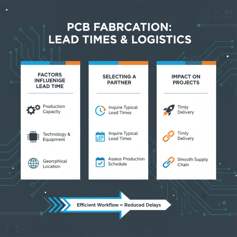
Lead Times and Logistics: Factors Affecting Delivery and Supply Chain
When selecting a PCB fabrication partner for your electronic projects, understanding lead times and logistics is crucial for ensuring timely delivery and a smooth supply chain. Lead times can vary significantly between manufacturers, influenced by factors such as their production capacity, technology, and geographical location. A partner with a robust production schedule and efficient workflow can drastically reduce the time it takes to receive your PCBs. It’s essential to inquire about their typical lead times and any potential delays that could arise due to demand fluctuations or resource availability.
Additionally, logistics play a vital role in the overall delivery process. The choice of shipping methods, transportation routes, and customs clearance procedures can all impact how quickly your PCBs arrive. Opting for a manufacturer with a reliable logistics network can mitigate unforeseen delays. It's advisable to discuss shipping options and timelines upfront, as well as to consider local suppliers that can provide quicker turnaround times. Understanding these factors will help in making an informed choice when selecting the best PCB fabricator for your needs, ultimately ensuring that your projects stay on schedule.