10 Essential Tips for Designing Your Own Printed Circuit Board (PCB)
In the realm of electronics, the design and fabrication of a printed circuit board (PCB) stand as a critical foundational element. The global PCB market was valued at approximately $61 billion in 2020 and is projected to reach around $85 billion by 2026, according to a report by Allied Market Research. This robust growth highlights the increasing importance of PCBs in the electronics industry, where they serve as the backbone for everything from consumer electronics to complex aerospace applications. As technology continues to evolve, the demand for innovative PCB designs becomes more pronounced, emphasizing the need for engineers and hobbyists alike to grasp essential design principles.
Renowned PCB expert Dr. Jennifer Smith once stated, "Understanding the intricacies of printed circuit board design can streamline manufacturing processes and significantly enhance product reliability." This underscores the theme of our discussion, focusing on the vital considerations when embarking on PCB design. Whether you are a seasoned engineer or a DIY enthusiast, mastering these design techniques will not only improve your project outcomes but also pave the way for future innovations in the fast-paced world of electronics.
Understanding PCB Basics: Key Concepts and Terminology
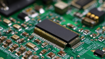
Understanding the basics of printed circuit boards (PCBs) is crucial for anyone looking to design their own boards. A PCB serves as the backbone for electronic devices, providing mechanical support and electrical connections for components.
Key terminologies in PCB design include layers, traces, vias, and pads. Layers refer to the different levels in a PCB, often with multiple layers involved in modern designs to accommodate complex electronics. Traces are the conductive pathways that connect components, while vias are the plated holes that enable connections between layers. Accurate understanding of these terms is fundamental, as flawed PCB designs can significantly hinder performance and reliability.
According to recent industry reports, the global PCB market is projected to grow to approximately $83 billion by 2026, driven by advancements in technology and an increasing demand for miniaturization in electronic devices. With the rise of the Internet of Things (IoT), the need for efficient PCB designs is more critical than ever. Designers must also be aware of factors such as impedance control and electronic noise, which can affect circuit performance. Emphasizing the need for thorough knowledge in these basic concepts not only enhances design accuracy but also ensures that the final product meets industry standards and consumer expectations.
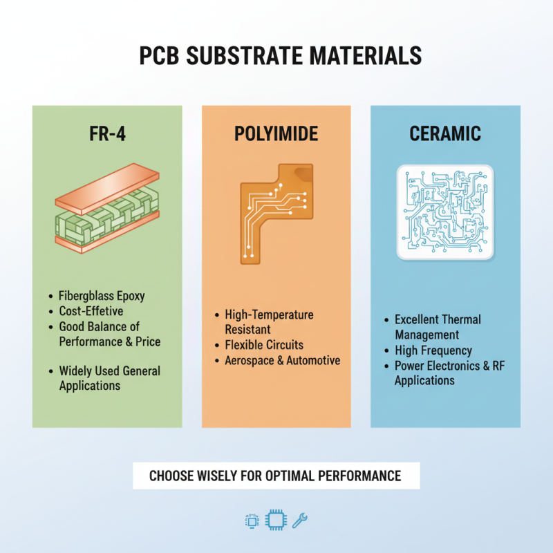
Choosing the Right Materials for PCB Fabrication: An Overview
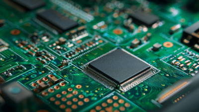
When designing your own printed circuit board (PCB), choosing the right materials for fabrication is crucial to ensure functionality and durability. The substrate material is one of the first considerations; common choices include FR-4, a widely used fiberglass epoxy, which balances cost and performance. Depending on the application, you may also consider materials like polyimide for high-temperature environments or ceramic substrates for enhanced thermal management. Each material has specific properties that can influence the performance of the PCB, so it’s important to match the material with the intended use.
Another essential aspect is the copper weight. Heavier copper layers can handle higher current loads, but they also increase fabrication costs and affect the thermal performance. For many designs, a standard copper weight is sufficient, but if your application involves high frequency or power, you should weigh the benefits of increased copper thickness.
Additionally, ensure that the surface finish you choose complements the operating environment of the PCB. Options like HASL provide good solderability, while OSP is often better for fine pitch components. By investigating and selecting the right materials at the beginning of the design process, you can significantly enhance the reliability and effectiveness of your PCB.
Design Software Selection: Top Tools Used in PCB Design
When embarking on the journey of designing your own printed circuit board (PCB), selecting the right design software is paramount. According to industry reports, over 70% of PCB designers cite software limitations as a leading cause of project delays. The right tool can streamline the design process, enhance collaboration, and mitigate errors. A well-chosen design platform provides advanced features such as real-time 3D visualization, effective routing algorithms, and easy integration with simulation tools, ultimately improving the quality and reliability of the final product.
To ensure successful PCB design, here are a few essential tips: Firstly, familiarize yourself with the software's user interface and functionalities through tutorials and online resources. This initial investment in learning can pay off significantly in increased efficiency. Secondly, leverage collaborative features available in many PCB design tools to involve team members early in the design process. Early feedback can help avoid costly revisions later. Lastly, always validate your design with simulation tools integrated within the software to identify potential issues before moving to production. This preliminary analysis is crucial, as industry studies have shown that about 40% of PCB manufacturing issues stem from oversights in the design phase.
Making informed software selections can significantly impact the success of your PCB projects. The right design tool not only enhances productivity but also ensures compliance with industry standards and supports innovation in design processes. Investing the time to evaluate and choose the right software can ultimately lead to more successful PCB designs and a quicker time to market.
10 Essential Tips for Designing Your Own Printed Circuit Board (PCB) - Design Software Selection: Top Tools Used in PCB Design
| Design Tool |
Key Features |
User Experience Level |
Cost |
| Eagle |
Easy to use, Massive library, Online design sharing |
Beginner to Intermediate |
Free for students, Paid plans start at $15/month |
| Altium Designer |
Advanced features, PCB design automation, Simulation capabilities |
Advanced |
Starts around $6,000 for a single license |
| KiCad |
Open-source, Extensive community support, 3D visualization |
Beginner to Advanced |
Free |
| Fusion 360 |
Cloud-based, Integrated CAD/CAM/CAE tools, Generative design |
Intermediate to Advanced |
Free for personal use, Paid plans start at $495/year |
| EasyEDA |
Web-based, Schematic and PCB integration, Community resources |
Beginner |
Free, with premium features available |
Best Practices for Layer Stackup and Circuit Routing Techniques
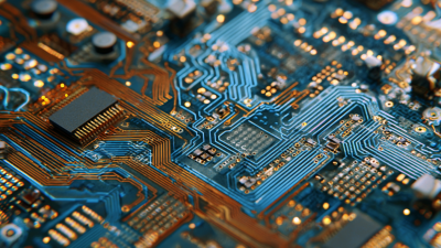
When designing your printed circuit board (PCB), layer stackup and circuit routing techniques are crucial for ensuring functionality, performance, and manufacturability. An effective layer stackup minimizes interference, optimizes signal integrity, and enhances thermal management. Aim for a strategic arrangement where power and ground layers are placed adjacent to signal layers, which helps reduce electromagnetic interference (EMI) and supports stable voltage levels across the board.
When it comes to circuit routing, keeping traces as short and direct as possible is essential for reducing resistance and inductance. Additionally, try to maintain consistent trace widths to prevent possible overheating. Implementing differential pairs for high-speed signals can also significantly improve performance by maintaining signal integrity and reducing noise. Furthermore, using vias judiciously can help in achieving efficient routing while avoiding unnecessary complexity.
Another tip is to consider the use of via stitching, which involves placing vias around critical components or areas to help manage grounding. This not only minimizes ground loops but also enhances the overall mechanical stability of the PCB. By following these best practices in layer stackup and routing techniques, you can create a well-designed PCB that meets both performance expectations and manufacturing standards.
Testing and Prototyping: Ensuring PCB Functionality Before Production
Testing and prototyping are critical stages in the development of a printed circuit board (PCB), ensuring that the design works as intended before mass production. Start by assembling a prototype of your PCB to validate its functionality. This prototype allows you to spot design flaws and make necessary adjustments. One key tip is to employ simulation software early in your design process to preemptively identify potential issues. Doing so can significantly reduce development time and costs associated with physical prototypes.
Once your prototype is ready, conduct thorough testing. This involves not just functional testing, but also thermal and mechanical reliability assessments. An essential tip here is to use a variety of test cases that simulate real-world conditions, including voltage variations and environmental changes. Additionally, involve different stakeholders in the testing phase, as their varied perspectives can lead to improvements that may not be obvious to the design team alone. By prioritizing rigorous testing and a comprehensive prototyping approach, you set the stage for a successful final product that meets both performance and reliability standards.
PCB Design Testing and Prototyping Success Rates