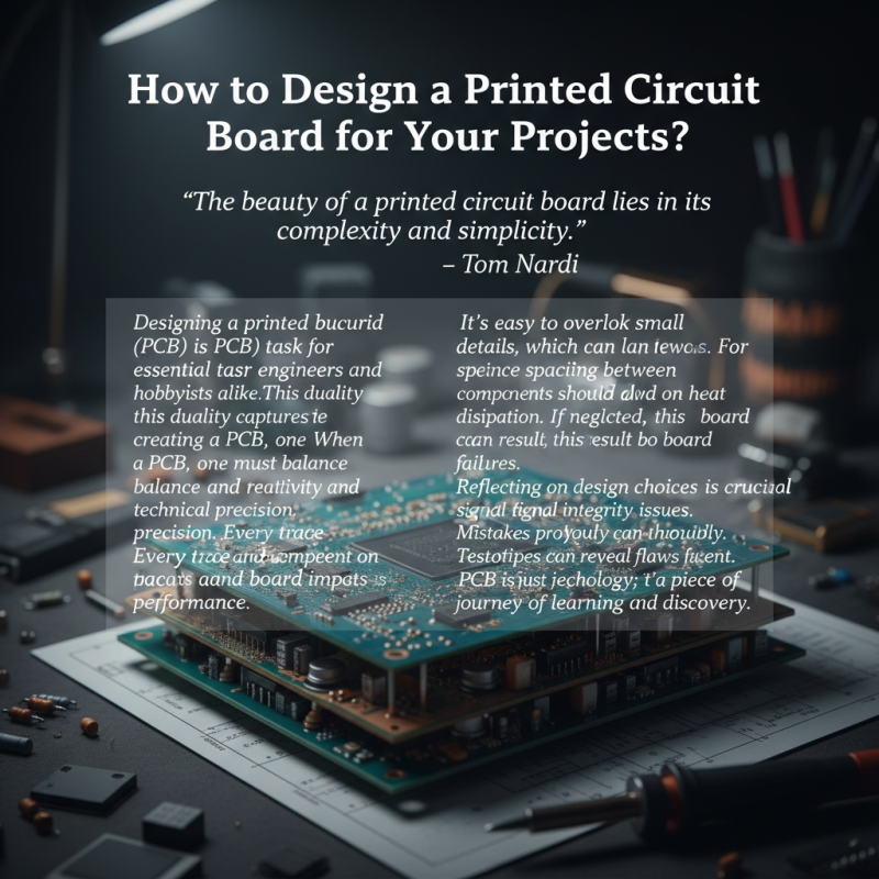
How to Design a Printed Circuit Board for Your Projects?
Designing a printed circuit board (PCB) is an essential task for engineers and hobbyists alike. Tom Nardi, a well-known expert in the PCB industry, once said, "The beauty of a printed circuit board lies in its complexity and simplicity." This duality captures the essence of PCB design.
When creating a PCB, one must balance creativity and technical precision. Every trace and component placement on the board impacts its performance. It's easy to overlook small details, which can lead to expensive reworks. For instance, spacing between components should allow for heat dissipation. If neglected, this can result in board failures.
Reflecting on design choices is crucial for improvement. Mistakes in layout can lead to signal integrity issues. Testing prototypes thoroughly can reveal flaws not initially apparent. A PCB is not just a piece of technology; it's a journey of learning and discovery.
Understanding the Basics of Printed Circuit Board (PCB) Design
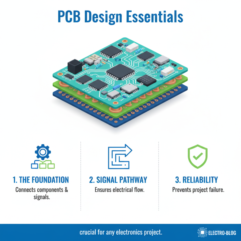
Understanding the design of printed circuit boards (PCBs) is crucial for any electronics project. A PCB is the foundation of your electronic device. It connects various components and provides a pathway for electrical signals. Without a solid design, your project can fail easily.
Begin by drafting a schematic. This diagram shows how each component interacts. It outlines connections but can become messy if not managed well. Start simple. Use clear symbols and labels. This will help reduce errors during assembly. Pay attention to spacing; overcrowded designs can lead to confusion and mistakes.
After creating the schematic, move to layout design. This step requires precision. Place components strategically to minimize trace lengths. However, avoid clutter and overlapping paths. Errors may arise if traces cross each other. Review your layout multiple times. Flaws in the design can lead to circuit problems later on. Adjust as necessary. Good designs often require revisions, and that’s perfectly acceptable.
Choosing the Right PCB Design Software for Your Project
When selecting PCB design software, the first step is to consider your project needs. Different projects require different features. For example, some designs may need advanced simulation capabilities, while others may focus on ease of use. According to a report by PCB Design Magazine, around 70% of engineers prioritize usability over extensive features when choosing software. This trend emphasizes the importance of a user-friendly interface.
Next, compatibility is a key factor. Many software options support various formats, but not all. Ensuring that your chosen software can import and export files with ease is crucial. A study by Digi-Key shows that 40% of engineers encounter issues due to incompatible file formats. This can lead to frustration and wasted time.
Additionally, consider the learning curve. Software should be intuitive to prevent delays. Reports indicate that engineers spend up to 30% of their project time learning new tools. It's important to find a balance between capabilities and ease of learning. Every tool has its quirks, and acknowledging that may improve your workflow efficiency.
Ultimately, the right PCB design software can significantly impact your success. It's worth taking the time to evaluate your options carefully.
Key Considerations for Schematic Capture and Layout
When designing a printed circuit board (PCB), schematic capture is crucial. This is where ideas become more tangible. You'll add components like resistors and capacitors. Connecting these correctly is vital. A mistake here can lead to circuit failures. Keep your layout clear. It should avoid clutter.
Considerations for layout follow closely behind. Pay attention to the placement of components. It affects electrical performance. Shorter traces can reduce interference. Utilize ground planes to stabilize voltage levels. However, it's easy to overlook the spacing of traces. Insufficient space can lead to short circuits. Check your designs frequently. Mistakes are a natural part of the process.
Revisiting your work is essential. You'll spot details that need refinement. Each iteration should improve the layout. Think about thermal management too. Components generate heat, and proper placement helps. Don’t forget about accessibility for soldering. Limiting yourself to specific formats can hinder creativity. Stay open to exploring different design patterns.
How to Design a Printed Circuit Board for Your Projects? - Key Considerations for Schematic Capture and Layout
| Aspect |
Description |
Considerations |
| Schematic Capture |
The process of creating the electrical diagram of the circuit. |
Ensure clear labeling and organization of components. |
| Component Selection |
Choosing suitable components based on specifications and availability. |
Consider power ratings, footprint, and thermal management. |
| Board Layout |
Arranging components on the PCB for optimal performance. |
Follow design rules for trace width and spacing. |
| Signal Integrity |
Maintaining the quality of electrical signals throughout the PCB. |
Minimize crosstalk and reflections through layout techniques. |
| Thermal Management |
Handling heat generated by components during operation. |
Incorporate heat sinks and proper ventilation in design. |
| Testing and Validation |
Evaluating the PCB performance against design specifications. |
Implement a thorough testing plan including functional and stress tests. |
Best Practices for Component Placement and Routing
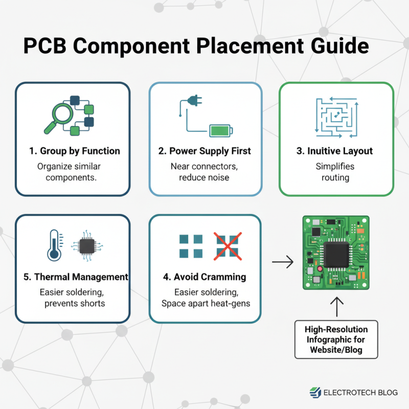
When designing a printed circuit board (PCB), component placement is critical. Start by grouping components with similar functions. Place power supply parts near connectors. This reduces noise in sensitive areas. Use an intuitive layout to simplify the routing process. Avoid cramming components tightly together. It can lead to difficulties during soldering. Also, prevent thermal issues. If components generate heat, space them apart.
Routing is equally important. Aim for shorter traces between components. This minimizes signal loss and interference. Use wider traces for higher currents. They can handle more heat with less resistance. Pay attention to ground paths; a solid ground plane enhances stability. Sometimes, your routing plan may look cluttered. Don't hesitate to revise it. Keep an eye out for potential bottlenecks. Simplifying a complex layout often improves performance.
As you develop your PCB, be mindful of the design tools. They may have specific limitations. It’s easy to overlook a mistake. Double-check for intersections and vias. These can create issues in production. Regularly reviewing your work helps catch errors before it’s too late. A good design evolves through iterations, not a single draft.
Finalizing Gerber Files and Preparing for Production
Designing a printed circuit board (PCB) involves several steps that culminate in finalizing the Gerber files. These files are essential for manufacturing your board. Ensure you double-check your design before exporting these files. A small error can lead to big problems in production.
Tips: Create a checklist of design rules. This includes trace width, pad sizes, and component placements. It helps catch mistakes early. Consider using design software with built-in validation tools to streamline this process.
After validating, export your Gerber files in the correct format. Each layer of the PCB needs a separate file. Consider including files for silkscreen layers and solder mask. Mistakes in this stage can delay production and increase costs.
Tips: Be meticulous. Review each layer against your design. Sometimes, having a fresh set of eyes can uncover issues you missed. Don’t hesitate to ask for feedback from peers. Reflections on your design can lead to necessary improvements.