Circuit board design turns an electrical concept into a manufacturable physical system. It defines where components sit, how copper traces connect them, and how signals travel through layered material. A designer balances performance, cost, safety, assembly, and future maintenance. The work begins with a schematic. It ends with verified manufacturing files.
The scale is substantial. Prismark’s 2024 PCB Industry Forecast Report tracks continued demand from automotive electronics, data centers, communications, and advanced computing. IPC’s International Technology Roadmap for Printed Circuit Boards also highlights rising layer counts, tighter geometries, improved power delivery, and stronger reliability requirements. These trends make circuit board design more than simple trace routing. A high-speed memory line may need controlled impedance. A power stage may require wide copper pours, thermal vias, and carefully measured clearances. One small connector can affect the entire layout.
Good practice depends on evidence, not visual confidence. Engineers review design rules, run electrical checks, inspect thermal behavior, and compare prototypes against test results. Standards from IPC provide widely recognized guidance for materials, fabrication, and assembly. Yet no tool catches everything. A simulation may miss a connector problem. A prototype may reveal unexpected noise near a switching regulator. That is normal, although it deserves reflection. Effective design therefore combines software, standards, laboratory measurements, and manufacturing feedback. This article explains how the process works, from requirements and schematic capture to layout, testing, and production release.
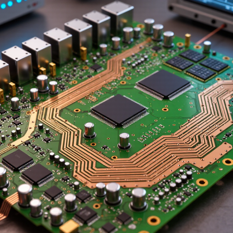
Circuit board design is the process of turning an electrical idea into a dependable physical system. It defines where components sit, how signals travel, and how power reaches each circuit. The work matters because a small layout decision can affect safety, speed, heat, and repair time.
A skilled designer studies the circuit diagram before placing parts. Sensitive signal paths may need short, direct routes. Power traces often require more width to handle current without excessive heating. Clearances also matter. Two copper areas placed too closely can create faults during manufacturing or use. A practical review checks the board layer by layer, like inspecting streets on a detailed map.
Physical details reveal hidden problems. A connector near the edge improves access. Test points help technicians measure voltage without damaging components. Ventilation space can prevent heat from collecting beneath a processor. Design software can flag many errors, but it cannot understand every real-world condition. That is where engineering judgment matters. No design is perfect. A rushed prototype may work once, then fail after vibration, moisture, or repeated heating. Careful testing should challenge the board under realistic conditions, while documented measurements support reliable decisions. Sometimes the overlooked detail matters most.
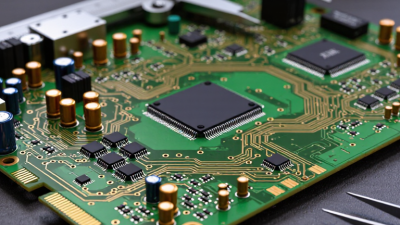
What Is Circuit Board Design and How Does It Work?
The Main Parts and Layers of a Circuit Board
Circuit board design arranges electrical paths, components, and mechanical features on a compact platform. In practical work, engineers begin with a substrate, usually a rigid insulating material that supports the board. Copper traces carry signals between resistors, capacitors, processors, connectors, and other components. Pads provide soldering points, while vias connect copper paths between different layers. The solder mask protects exposed copper and reduces accidental contact. A printed identification layer marks component locations and reference labels.
Most boards contain several copper layers separated by insulating material. The outer layers hold components and visible routing. Inner layers often carry power and ground planes, creating shorter and more stable electrical paths. Vias pass signals vertically through the stack. This layered structure saves space and can reduce noise when designed carefully. Small errors matter. A misplaced via may block a trace, weaken signal quality, or complicate assembly. Design software helps, but human review remains essential.
Tips: Keep high-speed traces short and direct. Separate sensitive signal paths from noisy power routes. Check clearances before manufacturing. Review the layer stack with an experienced engineer. I sometimes find that an early layout looks efficient but creates thermal or repair problems later, so practical inspection should challenge the first design.
Copper layers carry electrical current and signals through a circuit board. A common reference is 1 ounce of copper, which is approximately 35 micrometers thick when uniformly distributed across one square foot. Outer layers may use thicker copper when higher current capacity is required, while inner signal layers are often thinner to support controlled impedance and compact routing.
What Is Circuit Board Design and How Does It Work?
Circuit board design turns an electrical schematic into a physical, manufacturable board. A schematic shows connections, but not physical distance, heat, or mechanical limits. The designer first confirms component footprints, pin assignments, power requirements, and signal directions. Each symbol must match its real package. A small mismatch can stop an otherwise correct circuit.
The layout process places components on the board, then routes copper traces between them. Power paths usually need wider traces, while sensitive signals may require short, controlled routes. Ground planes can reduce noise and provide a stable return path. Designers also check spacing, layer thickness, impedance, and heat flow. Design-rule checks catch many errors, but they cannot replace engineering judgment. A connector may fit electrically yet fail when a cable pulls against the enclosure. This happens more often than expected.
Tips: Review the schematic before routing. Group related components together. Keep decoupling capacitors close to power pins. Label test points clearly. Print the board outline at full scale and check the mounting holes by hand. A second review is valuable, especially around power and high-speed signals. No layout is perfect. Some design choices still require testing, measurement, and thoughtful revision.
| Design Stage | Primary Input | Typical Activities | Key Output | Important Checks |
|---|---|---|---|---|
| 1. Requirements Definition | Electrical, mechanical, environmental, and regulatory requirements |
|
Design specification and acceptance criteria | Power limits, enclosure size, connector locations, operating conditions, and applicable safety requirements |
| 2. Electrical Schematic | Functional requirements and circuit architecture |
|
Logical circuit representation | Correct connectivity, power symbols, ground connections, component values, and unconnected-pin review |
| 3. Component Selection | Approved circuit functions and performance targets |
|
Bill of materials and chosen footprints | Voltage rating, current rating, tolerance, power dissipation, package dimensions, lifecycle, and sourcing risk |
| 4. PCB Stack-Up Planning | Signal speed, power requirements, board thickness, and layer constraints |
|
Layer stack-up and fabrication rules | Manufacturable layer spacing, dielectric thickness, impedance targets, thermal needs, and total board thickness |
| 5. Component Placement | Imported schematic, footprints, enclosure model, and interface requirements |
|
Preliminary physical arrangement | Orientation, serviceability, heat sources, airflow, creepage, clearance, mounting holes, and component height |
| 6. Trace Routing | Placed components, net classes, and design rules |
|
Connected copper layout | Trace width, current capacity, spacing, return paths, differential-pair matching, via usage, and impedance control |
| 7. Power and Ground Integrity | Power-distribution requirements and load estimates |
|
Stable power-distribution network | Voltage drop, current density, return-current paths, plane continuity, transient response, and thermal rise |
| 8. Design Rule Checking | Completed layout and configured electrical and manufacturing rules |
|
Validated layout database | Minimum trace width, minimum spacing, annular ring, drill limits, copper-to-edge clearance, and net completeness |
| 9. Signal and Thermal Analysis | Critical nets, operating frequencies, power dissipation, and material data |
|
Performance-optimized layout | Overshoot, ringing, crosstalk, timing margin, impedance, temperature rise, and electromagnetic compatibility risks |
| 10. Manufacturing Documentation | Approved schematic, PCB layout, and component data |
|
Manufacturing package | Fabrication drawings, assembly drawings, drill data, solder-paste data, pick-and-place data, and revision control |
| 11. Prototype and Testing | Manufactured prototype boards and test procedures |
|
Test results and engineering changes | Continuity, insulation, functional performance, thermal behavior, mechanical fit, and compliance-related tests |
| 12. Revision and Release | Test findings, design reviews, and approved changes |
|
Production-ready PCB design | Matched schematic and layout revisions, updated bill of materials, resolved issues, approval status, and archived source files |
Circuit board design turns an electrical idea into a manufacturable physical layout. The work begins with requirements: voltage, current, dimensions, operating temperature, and safety limits.
A 2024 market analysis valued the global PCB market at about $89.7 billion in 2023. That scale reflects rising demand for disciplined design practices.
Engineers then draw the schematic and assign suitable components. Each symbol must match a real package, footprint, and available specification. I always check pin numbers twice. A single swapped connection can damage an otherwise correct prototype.
Next, the layout places critical parts close together, especially power devices, processors, and decoupling capacitors. Signal paths are routed with controlled spacing, grounding, and impedance in mind. Thermal areas need copper, vias, and enough airflow.
Design-rule checks catch clearance, width, and connectivity errors. However, software cannot judge every practical weakness. A board may pass digitally yet fail during assembly or vibration testing.
Engineers review fabrication limits under IPC-2221 guidance, then release manufacturing files for prototype production. Testing measures voltage rails, noise, temperature, and functional performance.
The 2024 Global E-waste Monitor reported 62 million tonnes of electronic waste in 2022, with only 22.3% formally recycled.
Designers should therefore question unnecessary layers, difficult repairs, and material choices before production. Some decisions still require compromise.
Circuit board testing begins before the first panel reaches the factory floor. Engineers review the schematic, layout, layer stack, and component clearances. They check trace widths, drill sizes, solder-mask openings, and controlled-impedance paths. A practical review also compares the design with the manufacturer’s process limits.
Manufacturing preparation converts design data into usable production files. These usually include copper layers, solder-mask layers, silkscreen files, drill data, and fabrication notes. Engineers panelize several boards to reduce material waste and improve machine efficiency. They also define surface finishes, board thickness, tolerances, and inspection requirements. Small errors matter. An omitted drill note can delay an entire build.
Testing should occur at several stages. Bare boards may receive automated electrical testing for opens and shorts. During assembly, optical inspection checks component placement, polarity, solder bridges, and missing parts. X-ray inspection can examine hidden joints beneath dense packages. Functional testing then applies power and verifies real operating behavior. Test fixtures need stable contact, clear limits, and documented results.
Traceability links each board to its revision, materials, inspection records, and operator checks. A test fixture may fit perfectly on paper and fail on the bench. That gap deserves investigation, not excuses. No process is flawless. Engineers should review unexpected failures, adjust the design or process, and repeat validation before approving larger production runs.