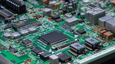
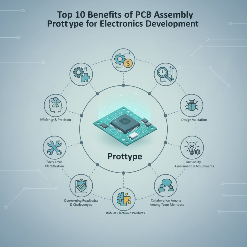
Top 10 Benefits of PCB Assembly Prototype for Electronics Development?
In the fast-paced world of electronics development, the demand for efficiency and precision is critical. One of the key components in this process is the "pcb assembly prototype." This prototype serves as a tangible model, allowing engineers to test and refine their designs before full-scale production. Integrating prototypes into the development cycle saves both time and costs.
A pcb assembly prototype enhances design validation. It provides an early glimpse into potential issues and helps identify errors. Engineers can assess functionality and make necessary adjustments. However, not every prototype is perfect. Issues can arise, requiring teams to rethink their designs. This iterative process fosters creativity and innovation, as mistakes often lead to valuable lessons.
Additionally, using a pcb assembly prototype fosters collaboration among team members. It encourages discussions and diverse input, which can spark new ideas. While roadblocks may present challenges, they also offer opportunities for improvement. Embracing imperfections in prototypes can ultimately lead to more robust electronic products. The benefits of utilizing such prototypes in electronics development are profound and multifaceted.
Benefits of Rapid Prototyping in PCB Assembly for Electronics
Rapid prototyping in PCB assembly
is a game-changer for electronics development. This approach allows engineers to
quickly create and test prototypes, accelerating the design cycle. According to a
recent industry report, companies using rapid prototyping can reduce their product
development time by up to 50%.
This efficiency is crucial in a competitive market where speed to market can
determine success.
The ability to iterate designs rapidly means that flaws can be identified
earlier. Testing a prototype often uncovers issues that wouldn't appear in simulations.
Industry data shows that 40% of
projects face delays due to design errors. By utilizing rapid prototyping, teams can
refine their designs effectively. This leads to a reduction in manufacturing costs, as
fewer revisions are needed during the assembly phase.
Moreover, rapid prototyping encourages innovation.
Designers can experiment with different materials and layouts without significant
investment. However, this flexibility can lead to analysis paralysis. Not every
prototype needs to be perfect. Some may only serve to explore ideas, and that’s okay.
The goal is to learn and adapt quickly. Balancing speed and
thoroughness remains a challenge for many
teams in the field.
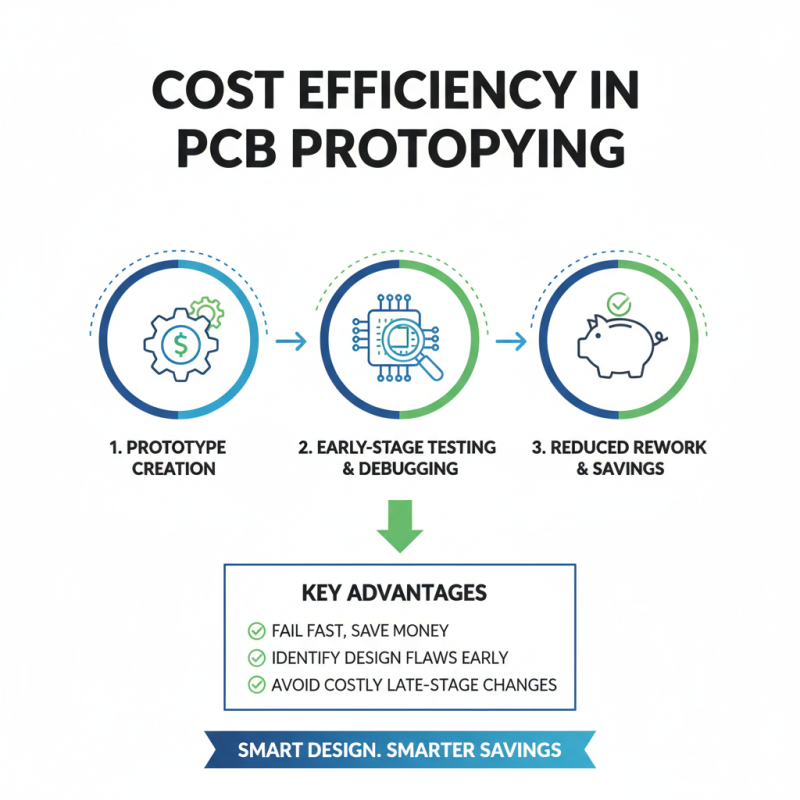
Cost Efficiency in PCB Prototype Development and Testing
Cost efficiency is a significant advantage of PCB prototype development. Creating prototypes allows developers to test designs without committing to mass production. Early-stage testing helps identify design flaws. This process can save money in the long run, reducing extensive rework costs that occur in later stages.
Additionally, using prototypes speeds up the overall development timeline. Engineers can quickly iterate on their designs. Faster turnaround enhances innovation. However, some teams underestimate the time needed for thorough testing before moving forward. This oversight can lead to unexpected expenses down the line.
Prototyping also lowers material waste. By validating a concept before full-scale production, companies only use necessary resources. Yet, investing in high-quality prototypes may seem costly initially. This hesitance might delay decision-making and lead to missed market opportunities. Balancing short-term costs with long-term benefits is crucial for every project.
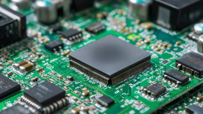
Improved Design Validation through PCB Prototyping
Prototyping is crucial in electronics development. It allows designers to create physical models of their ideas. This process helps identify flaws early in the design phase. When you hold a prototype, you see issues that aren’t apparent on paper. For instance, component placement may seem fine in CAD software. However, in a real prototype, you might discover spacing problems.
Moreover, a PCB prototype offers a tangible way to test functionality. You can run simulations and troubleshoot. This isn’t just about checking if it works. You may notice unexpected behaviors or integration issues. For example, a sensor may not respond correctly to stimuli. This experience prompts designers to refine their approach. Reflection on these challenges often leads to innovative solutions.
Validation through prototyping accelerates the development cycle. While you make adjustments, you also gain insights into market demands. Collecting feedback from potential users early is important. This interaction may reveal preferences that shift your design direction. Overlooking user input can lead to wasted resources. Each prototype iteration teaches vital lessons for the final product.
Top 10 Benefits of PCB Assembly Prototype for Electronics Development
Accelerated Time-to-Market with PCB Assembly Prototypes
In the fast-paced electronics sector, PCB assembly prototypes speed up time-to-market. According to industry reports, companies that use prototypes can reduce development time by 30%. This acceleration permits teams to test and refine concepts quickly. A shorter timeline translates to faster product launches and improved competitiveness.
Creating prototypes facilitates better iteration. Early testing identifies design flaws not visible in CAD models. Engineers can pivot easily based on real-world performance. Data indicates that rapid prototyping improves the likelihood of product success by up to 50%. However, rushing through prototypes can lead to overlooked issues, demanding thoughtful reflection on design choices.
Tips for effective PCB assembly prototyping include focusing on key components first. Prioritize what impacts functionality most. Ensure to conduct thorough testing after each iteration. Involve cross-functional teams to gain diverse insights. These steps can maximize the value of prototypes while minimizing potential risks. Remember, each prototype is a learning opportunity, so embrace imperfections.
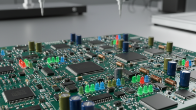
Enhanced Customization and Flexibility in Electronics Design
In the rapidly evolving field of electronics, enhanced customization and flexibility are vital. PCB assembly prototypes allow designers to experiment with different configurations. This flexibility means they can adapt to changing requirements throughout the development process. Small adjustments to the layout can be made easily, leading to more efficient designs that meet specific needs.
A prototype can expose design flaws early. This early-stage testing helps in making informed decisions. The power to tweak components offers opportunities to innovate, but it also requires constant reflection on choices made. Designers may find limitations they hadn't anticipated. Learning from failures is part of the process.
Moreover, a PCB prototype facilitates collaboration among teams. Different departments can input their specialized knowledge into the prototype design. This exchange fosters creativity but can also lead to conflicting ideas. Balancing various perspectives may not always be seamless. Ultimately, the goal is to create an optimized product that resonates with the target audience.