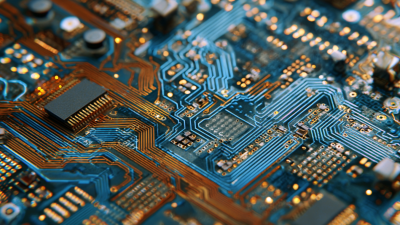
2026 Top Trends in PCB Printed Circuit Board Technology?
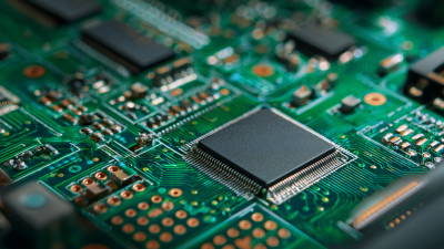
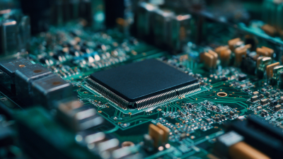
The future of technology is rapidly evolving, and so are the components that drive it. One key player in this evolution is the pcb printed circuit board. This essential component supports and connects various electronic elements. As we look toward 2026, several trends promise to reshape the landscape of pcb printed circuit board technology.
Innovation in materials is one trend to watch. Manufacturers are exploring new substances to enhance durability and performance. Flexible pcbs are gaining attention as devices become more compact. Another highlight involves automation in production. Automated processes promise to reduce errors and improve efficiency, yet they also challenge traditional manufacturing jobs.
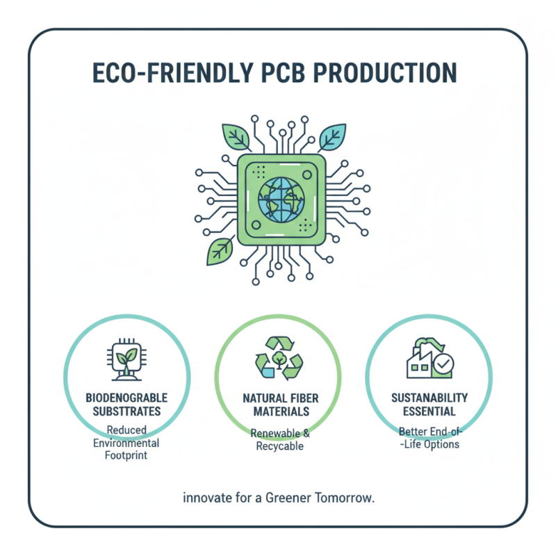
Moreover, sustainability continues to be a key concern. Eco-friendly practices in pcb printed circuit board production are becoming more commonplace. Companies must adapt or risk falling behind in a competitive market. Each trend brings potential benefits but also raises questions. How will these changes affect the industry as a whole? The journey towards 2026 will reveal the answers.

Emerging Materials Advancements in PCB Technology by 2026
The future of PCB technology looks promising, especially with advancements in materials. By 2026, we expect to see a significant shift towards eco-friendly materials. Traditional substrates might be replaced with biocompatible alternatives. These new materials aim to reduce environmental impact while maintaining performance.
Another trend is the development of flexible materials. Flexible PCBs can adapt to various shapes and environments. This transforms how circuit boards are deployed in various devices, enhancing their usability. However, not all flexible materials offer the same durability. Finding the right balance between flexibility and reliability remains a challenge.
Conductive inks also play a crucial role in this evolution. Printed electronic components can be produced using advanced inks. These inks enable lightweight and compact designs, leading to more efficient devices. Yet, quality control in production is essential. Inconsistent ink quality could undermine performance. New testing methods will be vital to ensure reliability and performance in these emerging technologies.
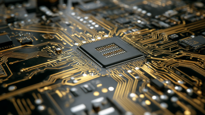
Miniaturization Trends in Printed Circuit Boards for Compact Devices
The trend of miniaturization in printed circuit boards (PCBs) is gaining momentum. Competing in a compact world pushes manufacturers to create smaller, yet powerful devices. Consumers expect more functionalities without added bulk. This expectation drives innovation in PCB technology.
To achieve miniaturization, PCB designs are becoming increasingly intricate. Advanced materials and components are essential. Tiny capacitors and resistors are now commonplace. Techniques like via-in-pad and microvias enable designers to save space. However, this complexity can lead to challenges in manufacturing. Ensuring reliability becomes crucial when components are packed closely together.
Tips: Always consider thermal management. As devices get smaller, heat dissipation is a concern. Use heat sinks or thermal vias appropriately. Also, plan for easy repairs. Compact designs can complicate maintenance. Simplifying access to key components can enhance product lifespan. Balancing miniaturization with functionality is vital. It demands continuous design evaluation and testing. Embracing these challenges can lead to better, smaller devices.
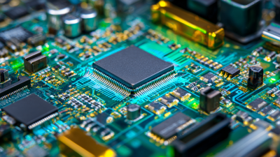
Integration of Smart Technologies in PCB Design and Manufacturing
The integration of smart technologies in PCB design and manufacturing is transforming the landscape of electronics. Intelligent systems can streamline workflows, reducing manual errors and increasing efficiency. Automated tools assist engineers in optimizing circuit layouts. This leads to improved performance in the final product. However, not all implementations are flawless. There can be compatibility issues during the integration process.
Utilizing smart technologies means embracing advanced simulations and real-time data analysis. These tools provide insights into performance and reliability. Designers can make data-driven decisions earlier in the development phase. Despite these benefits, some challenges persist. Not every team has access to the latest technologies, which can hinder progress. The learning curve can also be steep for new tools.
As the industry evolves, it faces the need for skilled professionals. Training programs must adapt to include smart technology applications. Companies often struggle to keep their teams updated. There is a risk of falling behind if they don’t invest in continuous education. Overall, while integrating smart technologies offers great potential, careful consideration is essential to navigate its complexities.
2026 Top Trends in PCB Printed Circuit Board Technology
| Trend |
Description |
Impact on Industry |
Projected Growth Rate |
| Integration of AI |
Incorporating artificial intelligence in design processes to optimize layouts and improve yield. |
Enhances design efficiency and reduces time-to-market. |
15% |
| Flexible PCBs |
Development of flexible printed circuit boards for applications in wearable technology. |
Allows for innovative product designs with reduced weight. |
20% |
| High-Frequency PCBs |
PCBs designed to handle high-speed signals for telecommunications and RF applications. |
Improves performance in communication devices. |
10% |
| Sustainability in Manufacturing |
Adoption of eco-friendly materials and waste-reduction practices in PCB production. |
Promotes a greener manufacturing process and customer appeal. |
12% |
| 3D Printing for Prototyping |
Utilizing 3D printing technologies to create quick prototypes of PCBs. |
Reduces lead times and costs in the prototyping phase. |
18% |
Innovations in Thermal Management Techniques for PCBs in 2026
In 2026, innovations in thermal management techniques for PCBs will take center stage. Efficient heat dissipation is crucial in modern electronics, especially in densely packed devices. According to a recent industry report, 70% of PCB failures are due to thermal issues. As components become smaller and more powerful, managing heat is increasingly complex.
Advanced materials like graphene and thermal interface materials (TIMs) will become more widely used. These materials help dissipate heat faster than traditional methods. The shift toward printed electronics will also allow for better thermal distribution on PCBs. Research shows that these innovations could enhance performance by up to 30%.
Tips: Consider employing simulation tools to predict thermal behavior in your designs. Use multiple layers or vias to improve heat transfer. Regularly review your material choices; sometimes, older materials may offer better reliability. With careful planning, thermal management can be a hassle-free aspect of PCB design.
Yet, some challenges remain. Many engineers still lack adequate knowledge of new techniques. A gap in understanding advanced materials can lead to suboptimal designs, resulting in overheating and device failure. Continuous education and testing are essential to bridge this gap.