2025 Guide: How to Design PCB Effectively for Beginners and Professionals
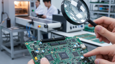
Designing a printed circuit board (PCB) is a crucial skill for both beginners and professionals in the electronics industry. As technology advances, the need for effective PCB design becomes more pronounced. Experts agree that mastering this process can significantly impact the performance and reliability of electronic devices. According to Dr. Emily Roberts, a renowned PCB design engineer, "A well-designed PCB can make the difference between a successful product and a costly failure." This statement underscores the importance of understanding the intricacies involved in the design PCB process.
In this guide, we will explore the fundamental principles of PCB design and provide actionable tips to help both novices and seasoned professionals enhance their skills. By following best practices and leveraging the right tools, individuals can streamline the design process, reduce errors, and ultimately produce high-quality PCBs. From schematic creation to layout optimization, understanding the nuances of how to design PCB effectively is essential for achieving desired outcomes in today's competitive tech landscape.

Understanding the Basics of PCB Design for Beginners
Understanding the basics of PCB design is crucial for both beginners and professionals aiming to create effective electronic circuits. The global printed circuit board market is projected to reach $100 billion by 2025, according to a report by Research and Markets. This growth highlights the increasing importance of PCB design in modern electronics, emphasizing the need for quality and innovation within this field. For beginners, mastering the fundamentals—such as understanding schematic diagrams, component placement, and the significance of routing—is essential for developing viable products.
A key aspect of PCB design involves the selection of materials and manufacturing techniques. For instance, using high-frequency laminates for RF applications or flexible substrates for compact devices can drastically influence performance. A study by IPC indicated that approximately 30% of PCB failures stem from poor design choices made early in the development process. This statistic underscores the importance of thorough design practices, including considering thermal management and electromagnetic interference, to enhance the longevity and reliability of electronic devices.
As designers refine their skills, they can utilize simulation tools to test and optimize their layouts, which is invaluable for reducing costly iterations and improving overall product quality.
Essential Tools and Software for PCB Designing
When embarking on the journey of PCB design, having the right tools and software is essential for both beginners and experienced professionals. The effectiveness of the design process heavily relies on the capabilities of these tools, which can streamline workflows and enhance accuracy.
Fundamental tools include schematic capture software, which allows designers to create circuit schematics, and PCB layout programs that facilitate the arrangement of components on the board while adhering to industry standards.
These tools help in visualizing the project and make it easier to detect errors early in the design phase.
In addition to traditional design software, simulation tools play a crucial role in verifying the functionality and performance of the PCB before manufacturing. These applications allow designers to run tests and analyze electrical characteristics under various conditions, ensuring the reliability of the final product.
Collaboration software is also vital, enabling teams to work together seamlessly, regardless of location.
Features like version control and real-time feedback greatly enhance communication and reduce the risk of errors during the design process.
By leveraging these essential tools and software, designers can create efficient, high-quality PCB layouts that are both innovative and practical.
Key Principles of Effective PCB Layout and Routing
The effectiveness of a printed circuit board (PCB) layout can significantly influence the performance and reliability of electronic devices. Key principles of effective PCB layout and routing involve optimizing component placement, ensuring minimal electromagnetic interference (EMI), and maintaining signal integrity. According to the 2022 IPC A-600 report, over 70% of electronic device failures can be traced back to poor PCB design, making it imperative for both beginners and professionals to adhere to best practices in PCB design.
One fundamental principle is to strategically place components to minimize trace lengths while avoiding impedance mismatches. This not only reduces signal degradation but also mitigates the risk of crosstalk between adjacent traces. A study by the IEEE revealed that adhering to proper spacing guidelines can reduce EMI by up to 30%, providing a more reliable operation in high-frequency applications. Additionally, the routing of traces should prioritize a clear ground plane and incorporate via design techniques to ensure the thermal management of components, thus enhancing long-term reliability.
Moreover, it is crucial to incorporate design rules such as adequate trace width for current carrying and layered stack-ups to prevent ground loops. According to a recent report by the Design Automation Conference, designs that followed strict layout guidelines showed an 80% increase in product performance and lifecycle efficiency. By applying these principles, engineers can create PCBs that not only meet industry standards but also stand the test of time in real-world applications.
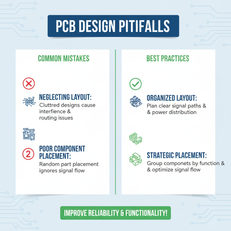
Common Mistakes to Avoid in PCB Design
When designing PCBs, beginners and professionals alike can fall into common pitfalls that undermine the functionality and reliability of their projects. One significant mistake is neglecting the importance of layout. A cluttered design can lead to interference and difficulty in routing. It’s essential to create a clear and organized layout, ensuring that components are placed strategically based on signal flow and power distribution.
**Tips:** Always start your design with a schematic that details component connections. Use ground and power planes to minimize interference and improve signal integrity. It’s also beneficial to regularly validate your design through simulation software, which can help identify potential issues before manufacturing.
Another prevalent error is overlooking proper trace width calculations. Traces that are too narrow can lead to overheating and potential failure, especially if they’re carrying significant current. Utilizing online calculators for trace width based on current capacity and temperature rise can significantly enhance the reliability of your PCB.
**Tips:** Consult industry standards for trace width depending on your design's specifications. Double-check your calculations to ensure that your traces can handle the expected loads. Additionally, consider using wider traces or multiple layers if high currents are involved.
Testing and Prototyping: Ensuring Design Success
Prototyping and testing are crucial steps in the PCB design process that can save time and resources in the long run. For beginners, creating a prototype allows for the exploration of your design without the commitment of full-scale production. It provides the opportunity to identify potential issues early, ensuring that modifications can be made before finalizing the design. Often, this stage involves building a simple version of your PCB that can be tested for functionality and reliability.
**Tips:** When prototyping, use breadboards for rapid testing of circuits. This not only helps in verifying the design but also allows you to make quick adjustments. Start with basic components and gradually add complexity, which will help isolate any design flaws.
Once your prototype is ready, rigorous testing is the next step. This involves assessing the performance of the PCB under various conditions to ensure it meets the required specifications. Factors to consider include thermal performance, signal integrity, and component compatibility. Documenting the results of these tests will provide insights into the design's strengths and weaknesses.
**Tips:** Develop a checklist of parameters to test for each prototype iteration. Utilize automated testing tools where possible, as they can greatly increase accuracy and efficiency in identifying issues.
PCB Design Success Metrics for 2025
This bar chart illustrates the key metrics involved in effective PCB design for 2025. It presents the average prototyping time, testing duration, number of design iterations, success rate of designs, and budget utilization. The data reflects essential areas for PCB designers to focus on, ensuring successful outcomes in their projects.